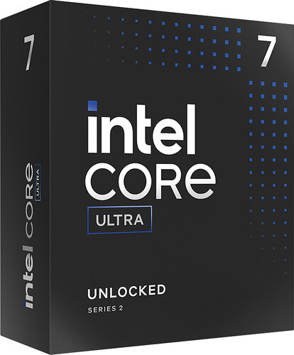
Intel Core Ultra 7 265K vs Intel Core i5-2415M
Intel Core Ultra 7 265K
$404
Intel Core i5-2415M
|
20 Cores
20 Threads
3.9GHz Clock
|
2 Cores
4 Threads
2.3GHz Clock
|
|
Socket
LGA 1851
|
Socket
BGA 1023
|
|
iGPU
Graphics 4C 2000MHz
2.05 TFLOPS FP32
|
iGPU
HD 3000 1200MHz
230 GFLOPS FP32
|
|
Manufacturer
Intel
|
Manufacturer
Intel
|
|
Architecture
Arrow Lake
|
Architecture
Sandy Bridge
|
|
Family
Core Ultra Series 2
|
Family
Core 2nd Gen
|
|
Instruction Set (ISA)
x86-64
|
Instruction Set (ISA)
x86-64
|
|
Codename
-
-
Arrow Lake-S-8P-16E
P-Core
Lion Cove
-
-
E-Core
Skymont
|
Codename
Sandy Bridge
Sandy Bridge-H-2
Sandy Bridge-2C-GT2
-
-
-
-
-
-
|
|
Market Segment
Desktop
|
Market Segment
Laptop
|
|
Release Date
10/24/2024
|
Release Date
1/1/2011
|
|
Foundry
TSMC
TSMC (iGPU Die)
TSMC (SoC Die)
TSMC (IO Die)
|
Foundry
Intel
-
-
-
|
|
Node
N3B
N5 (iGPU Die)
N6 (SoC Die)
N6 (IO Die)
|
Node
32nm
-
-
-
|
|
Die Size
135 mm²
23 mm² (iGPU Die)
100 mm² (SoC Die)
28 mm² (IO Die)
|
Die Size
149 mm²
-
-
-
|
|
Transistor Count
Unknown
-
-
-
|
Transistor Count
624 Million
-
-
-
|
|
20 Cores
8 P-Cores
-
12 E-Cores
|
2 Cores
-
-
-
|
|
20 Threads
8 P-Threads
-
12 E-Threads
|
4 Threads
-
-
-
|
|
P-Core
3.9GHz
5.5GHz Boost
-
|
-
2.3GHz
2.9GHz Boost
-
|
|
-
-
-
|
-
-
-
|
|
E-Core
3.3GHz
4.6GHz Boost
|
-
-
-
|
|
Overclocking
Unlocked
-
-
-
|
Overclocking
Locked
-
-
-
|
|
Type
DMI
|
Type
DMI
|
|
-
-
|
-
-
|
|
-
-
|
-
-
|
|
Transfer Rate
16GT/s
|
Transfer Rate
5GT/s
|
|
-
-
|
-
-
|
|
Lanes
8
|
Lanes
4
|
|
Bandwidth
16GB/s
|
Bandwidth
2.5GB/s
|
|
Bi-directional
32GB/s
|
Bi-directional
5GB/s
|
|
L0 Instruction
-
-
|
L0 Instruction
-
-
|
|
L0 Data
-
-
|
L0 Data
-
-
|
|
L1 Instruction
64KB/P-Core
8-way set associative
-
-
64KB/E-Core
8-way set associative
|
L1 Instruction
32KB/Core
8-way set associative
-
-
-
-
|
|
L1 Data
48KB/P-Core
12-way set associative
-
-
32KB/E-Core
8-way set associative
|
L1 Data
32KB/Core
8-way set associative
-
-
-
-
|
|
L2
3072KB/Core
10-way set associative
-
-
-
-
-
-
-
-
12MB Shared (E-Core)
16-way set associative
|
L2
256KB/Core
8-way set associative
-
-
-
-
-
-
-
-
-
-
|
|
L3
-
30MB Shared
-
12-way set associative
-
-
-
-
-
|
L3
-
3MB Shared
-
12-way set associative
-
-
-
-
-
|
|
-
-
-
-
|
-
-
-
-
|
|
Channels
2
|
Channels
2
|
|
Max Memory
192GB
|
Max Memory
16GB
|
|
ECC
Supported
|
ECC
Not Supported
|
|
Bus Width/Channel
64Bit
Bus Width
128Bit
|
Bus Width/Channel
64Bit
Bus Width
128Bit
|
|
Clock
3200MHz
Transfer Rate
6400MT/s
|
Clock
667MHz
Transfer Rate
1333MT/s
|
|
Bandwidth/Channel
51.2GB/s
Bandwidth
102.4GB/s
|
Bandwidth/Channel
10.7GB/s
Bandwidth
21.3GB/s
|
|
TDP
125W
-
-
250W Peak
|
TDP
35W
-
-
-
|
|
Temp
105°C Max
-
|
Temp
100°C Max
-
|
|
Included Cooler
Not Included
|
Included Cooler
Not Included
|
|
PCIe 5.0 x20 Lanes
PCIe 4.0 x4 Lanes
|
PCIe 2.0 x16 Lanes
|
|
Graphics 4C 2000MHz
512 Shaders
2000MHz
2.05 TFLOPS FP32
|
HD 3000 1200MHz
96 Shaders
1200MHz
230 GFLOPS FP32
|
|
AI Boost 3
|
No NPU
-
|
|
-
2 Cores
|
-
-
|
|
13 TOPS INT8
|
-
|
|
-
-
|
-
-
|
|
No Cellular
|
No Cellular
|


Copy Link

