AMD Instinct MI100 vs AMD Radeon Instinct MI25
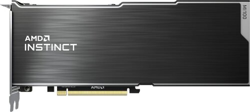
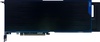
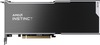
AMD Instinct MI100
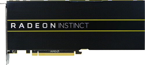
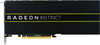
AMD Radeon Instinct MI25
|
7680 Shaders
32GB HBM2
1502MHz
|
4096 Shaders
16GB HBM2
1500MHz
|
|
Peak AI Performance
184.57 TFLOPS
FP16 Tensor (FP16 Accumulate)
|
Peak AI Performance
24.58 TFLOPS
FP16
|
|
FP32
23.07 TFLOPS
|
FP32
12.29 TFLOPS
|
|
FP16
46.14 TFLOPS
|
FP16
24.58 TFLOPS
|
|
Form Factor
PCIe Card
2.0-Slots
|
Form Factor
PCIe Card
2.0-Slots
|
|
TDP
300W
|
TDP
300W
|
|
Power Connectors
-
2x 8-Pin
-
-
|
Power Connectors
-
2x 8-Pin
-
-
|
|
GB6 Metal N/A
0%
|
GB6 Metal N/A
0%
|
|
GB6 Vulkan N/A
0%
|
|
GB5 OpenCL N/A
0%
|
GB5 OpenCL N/A
0%
|
|
GB5 CUDA N/A
0%
|
GB5 CUDA N/A
0%
|
|
GB5 Metal N/A
0%
|
GB5 Metal N/A
0%
|
|
GB5 Vulkan N/A
0%
|
GB5 Vulkan N/A
0%
|
|
OCT 2020.1 N/A
0%
|
OCT 2020.1 N/A
0%
|
|
OCT Metal N/A
0%
|
OCT Metal N/A
0%
|
|
Peak AI
Performance
184.57 TFLOPS
FP16 Tensor (FP16 Accumulate)
|
Peak AI
Performance
24.58 TFLOPS
FP16
|
|
-
-
-
|
-
-
-
|
|
-
-
-
-
-
-
|
-
-
-
-
-
-
|
|
FP16
46.14 TFLOPS
184.57 TFLOPS
Tensor (FP16 Accumulate)
-
184.57 TFLOPS
Tensor (FP32 Accumulate)
-
|
FP16
24.58 TFLOPS
-
-
-
-
|
|
FP32
23.07 TFLOPS
46.14 TFLOPS
Tensor
-
|
FP32
12.29 TFLOPS
-
-
|
|
FP64
11.54 TFLOPS
-
|
FP64
770 GFLOPS
-
|
|
BF16
-
92.28 TFLOPS
Tensor
-
|
-
-
-
-
|
|
-
-
-
|
-
-
-
|
|
INT4
92.28 TOPS
Tensor
-
|
-
-
-
|
|
INT8
-
92.28 TOPS
Tensor
-
|
-
-
-
-
|
|
-
-
|
-
-
|
|
-
-
|
-
-
|
|
Pixel
Fillrate
-
|
Pixel
Fillrate
96 GPixel/s
|
|
-
-
|
-
-
|
|
Texture
Fillrate
720.96 GTexel/s
|
Texture
Fillrate
384 GTexel/s
|
|
Manufacturer
AMD
|
Manufacturer
AMD
|
|
Chip Designer
AMD
|
Chip Designer
AMD
|
|
Architecture
CDNA 1
|
Architecture
GCN 5
|
|
Family
Instinct
|
Family
Instinct
|
|
Codename
Arcturus
-
Variant
Arcturus XL
|
Codename
Greenland
Vega 10
Variant
Vega 10 XT GL
|
|
Market Segment
Server
|
Market Segment
Server
|
|
Release Date
11/16/2020
|
Release Date
6/20/2017
|
|
Foundry
TSMC
-
|
Foundry
GlobalFoundries
-
|
|
Fabrication Node
N7
-
|
Fabrication Node
14LPP
-
|
|
Die Size
750 mm²
-
|
Die Size
486 mm²
-
|
|
Transistor Count
25.6 Billion
-
|
Transistor Count
12.5 Billion
-
|
|
Transistor Density
34.13M/mm²
-
|
Transistor Density
25.72M/mm²
-
|
|
Form
PCIe Card
|
Form
PCIe Card
|
|
Shading Units
7680 Shaders
-
|
Shading Units
4096 Shaders
-
|
|
Texture Mapping Units
480 TMUs
|
Texture Mapping Units
256 TMUs
|
|
Render Output Units
-
|
Render Output Units
64 ROPs
|
|
Tensor Cores
480 T-Cores
|
-
-
|
|
-
-
|
-
-
|
|
-
-
|
-
-
|
|
Compute Units
120 CUs
|
Compute Units
64 CUs
|
|
-
-
|
-
-
|
|
-
-
|
-
-
|
|
-
-
1000MHz Base
1502MHz
|
-
-
1400MHz Base
1500MHz
|
|
-
-
|
-
-
|
|
L1
-
-
16KB/CU
-
|
L1
-
-
16KB/CU
-
|
|
L2
8MB Shared
|
L2
4MB Shared
|
|
-
-
-
|
-
-
-
|
|
32GB
HBM2
ECC
|
16GB
HBM2
ECC
|
|
Bus Width
4096Bit
|
Bus Width
2048Bit
|
|
Clock
1200MHz
Transfer Rate
2.4GT/s
Bandwidth
1228.8GB/s
|
Clock
945MHz
Transfer Rate
1.9GT/s
Bandwidth
483.8GB/s
|
|
-
-
-
-
-
-
-
-
-
|
-
-
-
-
-
-
-
-
-
|
|
TDP
300W
|
TDP
300W
|
|
-
-
|
-
-
|
|
-
-
-
-
-
-
-
-
-
-
-
-
-
-
-
-
-
-
-
-
-
-
-
-
-
-
-
-
-
-
-
-
-
-
-
-
-
-
-
No Ports
|
-
-
-
-
-
-
-
-
-
-
-
-
-
-
-
-
-
1x mini-DisplayPort 1.4
-
-
-
-
-
-
-
-
-
-
-
-
-
-
-
-
-
-
-
-
-
|
|
Max Resolution
Unknown
|
Max Resolution
7680x4320
|
|
Max Resolution Refresh Rate
-
|
Max Resolution Refresh Rate
60Hz
|
|
Variable Refresh Rate
-
-
-
|
Variable Refresh Rate
-
FreeSync
-
|
|
Display Stream Compression (DSC)
Not Supported
|
Display Stream Compression (DSC)
Not Supported
|
|
Multi Monitor Support
Unknown
|
Multi Monitor Support
3
|
|
-
-
|
Content Protection
HDCP 2.2
|
|
Model
VCN 2.5
|
Model
VCE 4.0
|
|
Codec
-
-
-
-
-
-
-
-
AVC (H.264)
HEVC (H.265)
-
-
-
-
|
Codec
-
-
-
-
-
-
-
-
AVC (H.264)
HEVC (H.265)
-
-
-
-
|
|
Model
VCN 2.5
|
Model
UVD 7.0
|
|
Codec
MPEG-1
MPEG-2
MPEG-4
JPEG
VC-1
-
VP9
-
AVC (H.264)
HEVC (H.265)
-
-
-
-
|
Codec
MPEG-1
MPEG-2
MPEG-4
JPEG
VC-1
-
-
-
AVC (H.264)
HEVC (H.265)
-
-
-
-
|
|
-
-
-
-
|
Direct X
12
Direct 3D
12_1
|
|
-
-
OpenCL
2.1
-
-
|
OpenGL
4.6
OpenCL
2.1
Vulkan
1.3
|
|
-
-
-
-
GFX
9.4
-
-
-
-
|
Shader Model
6.7
-
-
GFX
9
-
-
-
-
|
|
-
-
-
-
|
-
-
-
-
|
|
Power Connectors
-
-
-
2x 8-Pin
-
-
-
|
Power Connectors
-
-
-
2x 8-Pin
-
-
-
|
|
Slots Required
2.0
PCIe Version
4.0
PCIe Lanes
16
|
Slots Required
2.0
PCIe Version
3.0
PCIe Lanes
16
|
|
Multi GPU Support
Supported
Type
Infinity Fabric
|
Multi GPU Support
Supported
Type
CrossFire XDMA
|
|
Height
111 mm (4.37 in)
Width
267 mm (10.51 in)
Depth
37 mm (1.46 in)
|
Height
111 mm (4.37 in)
Width
267 mm (10.51 in)
Depth
37 mm (1.46 in)
|


Copy Link