AMD Radeon Pro V620 vs NVIDIA Tesla P100
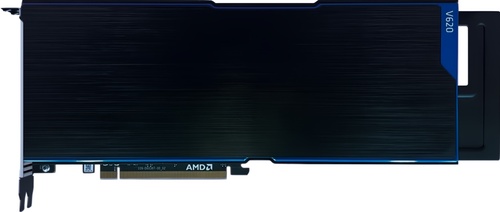
AMD Radeon Pro V620
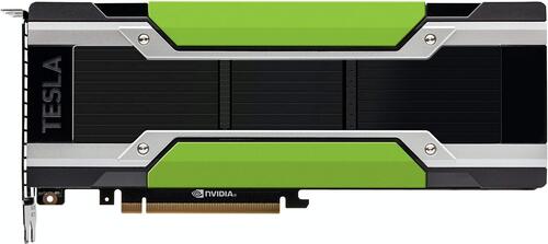
NVIDIA Tesla P100
$5,699
|
4608 Shaders
32GB GDDR6
2200MHz
|
3584 Shaders
16GB HBM2
1303MHz
|
|
Peak AI Performance
20.28 TFLOPS
FP32
|
Peak AI Performance
18.68 TFLOPS
FP16
|
|
FP32
20.28 TFLOPS
|
FP32
9.34 TFLOPS
|
|
-
-
|
FP16
18.68 TFLOPS
|
|
Form Factor
PCIe Card
2.0-Slots
|
Form Factor
PCIe Card
2.0-Slots
|
|
TDP
300W
|
TDP
250W
|
|
Power Connectors
-
2x 8-Pin
-
-
|
Power Connectors
-
1x 8-Pin
-
-
|
|
GB6 OpenCL N/A
0%
|
|
|
GB6 Metal N/A
0%
|
GB6 Metal N/A
0%
|
|
GB6 Vulkan N/A
0%
|
|
GB5 OpenCL N/A
0%
|
GB5 OpenCL N/A
0%
|
|
GB5 CUDA N/A
0%
|
GB5 CUDA N/A
0%
|
|
GB5 Metal N/A
0%
|
GB5 Metal N/A
0%
|
|
GB5 Vulkan N/A
0%
|
GB5 Vulkan N/A
0%
|
|
OCT 2020.1 N/A
0%
|
OCT 2020.1 N/A
0%
|
|
OCT Metal N/A
0%
|
OCT Metal N/A
0%
|
|
Peak AI
Performance
20.28 TFLOPS
FP32
|
Peak AI
Performance
18.68 TFLOPS
FP16
|
|
-
-
-
|
-
-
-
|
|
-
-
-
-
-
-
|
-
-
-
-
-
-
|
|
-
-
-
-
-
-
|
FP16
18.68 TFLOPS
-
-
-
-
|
|
FP32
20.28 TFLOPS
-
-
|
FP32
9.34 TFLOPS
-
-
|
|
FP64
1.27 TFLOPS
-
|
FP64
4.67 TFLOPS
-
|
|
-
-
-
-
|
-
-
-
-
|
|
-
-
-
|
-
-
-
|
|
-
-
-
|
-
-
-
|
|
-
-
-
-
|
-
-
-
-
|
|
-
-
|
-
-
|
|
-
-
|
-
-
|
|
Pixel
Fillrate
281.6 GPixel/s
|
Pixel
Fillrate
166.784 GPixel/s
|
|
-
-
|
-
-
|
|
Texture
Fillrate
633.6 GTexel/s
|
Texture
Fillrate
291.872 GTexel/s
|
|
Manufacturer
AMD
|
Manufacturer
NVIDIA
|
|
Chip Designer
AMD
|
Chip Designer
NVIDIA
|
|
Architecture
RDNA 2
|
Architecture
Pascal
|
|
Family
Radeon Pro V
|
Family
Tesla P
|
|
Codename
Sienna Cichlid
Navi 21
Variant
Navi 21 XL GL
|
Codename
NV130
GP100
Variant
GP100-893-A1
|
|
Market Segment
Server
|
Market Segment
Server
|
|
Release Date
11/4/2021
|
Release Date
6/20/2016
|
|
Foundry
TSMC
-
|
Foundry
TSMC
-
|
|
Fabrication Node
N7
-
|
Fabrication Node
16FF
-
|
|
Die Size
520 mm²
-
|
Die Size
610 mm²
-
|
|
Transistor Count
26.8 Billion
-
|
Transistor Count
15.3 Billion
-
|
|
Transistor Density
51.56M/mm²
-
|
Transistor Density
25.08M/mm²
-
|
|
Form
PCIe Card
|
Form
PCIe Card
|
|
Shading Units
4608 Shaders
-
|
Shading Units
3584 Shaders
-
|
|
Texture Mapping Units
288 TMUs
|
Texture Mapping Units
224 TMUs
|
|
Render Output Units
128 ROPs
|
Render Output Units
128 ROPs
|
|
-
-
|
-
-
|
|
-
-
|
-
-
|
|
-
-
|
Streaming Multiprocessors
56 SMs
|
|
Compute Units
72 CUs
|
-
-
|
|
-
-
|
-
-
|
|
-
-
|
-
-
|
|
-
-
1825MHz Base
2200MHz
|
-
-
1126MHz Base
1303MHz
|
|
L0
32KB/WGP
|
-
-
|
|
L1
-
-
-
128KB/Array
|
L1
-
64KB/SM
-
-
|
|
L2
4MB Shared
|
L2
4MB Shared
|
|
L3
128MB Shared
1.66TB/s
|
-
-
-
|
|
32GB
GDDR6
-
|
16GB
HBM2
-
|
|
Bus Width
256Bit
|
Bus Width
4096Bit
|
|
Clock
2000MHz
Transfer Rate
16GT/s
Bandwidth
512GB/s
|
Clock
715MHz
Transfer Rate
1.4GT/s
Bandwidth
732.2GB/s
|
|
-
-
-
-
-
-
-
-
-
|
-
-
-
-
-
-
-
-
-
|
|
TDP
300W
|
TDP
250W
|
|
-
-
|
-
-
|
|
-
-
-
-
-
-
-
-
-
-
-
-
-
-
-
-
-
-
-
-
-
-
-
-
-
-
-
-
-
-
-
-
-
-
-
-
-
-
-
No Ports
|
-
-
-
-
-
-
-
-
-
-
-
-
-
-
-
-
-
-
-
-
-
-
-
-
-
-
-
-
-
-
-
-
-
-
-
-
-
-
-
No Ports
|
|
Max Resolution
7680x4320
|
Max Resolution
Unknown
|
|
Max Resolution Refresh Rate
120Hz
|
Max Resolution Refresh Rate
-
|
|
Variable Refresh Rate
-
FreeSync
-
|
Variable Refresh Rate
G-Sync
FreeSync
-
|
|
Display Stream Compression (DSC)
Supported
|
Display Stream Compression (DSC)
Not Supported
|
|
Multi Monitor Support
4
|
Multi Monitor Support
Unknown
|
|
Content Protection
HDCP 2.3
|
-
-
|
|
Model
VCN 3.0
|
Model
3x NVENC 4
|
|
Codec
-
-
-
-
-
-
-
-
AVC (H.264)
HEVC (H.265)
-
-
-
-
|
Codec
-
-
-
-
-
-
-
-
AVC (H.264)
HEVC (H.265)
-
-
-
-
|
|
Model
VCN 3.0
|
Model
NVDEC 3
|
|
Codec
MPEG-1
MPEG-2
MPEG-4
JPEG
VC-1
-
VP9
-
AVC (H.264)
HEVC (H.265)
-
AV1
-
-
|
Codec
MPEG-1
MPEG-2
MPEG-4
-
VC-1
-
VP9
-
AVC (H.264)
HEVC (H.265)
-
-
-
-
|
|
Direct X
12
Direct 3D
12_2
|
Direct X
12
Direct 3D
12_1
|
|
OpenGL
4.6
OpenCL
2.1
Vulkan
1.2
|
OpenGL
4.6
OpenCL
3.0
Vulkan
1.3
|
|
Shader Model
6.7
-
-
GFX
10.3
-
-
-
-
|
Shader Model
6.0
CUDA
6.0
-
-
PureVideo HD
VP8
VDPAU
Feature Set H
|
|
-
-
-
-
|
-
-
-
-
|
|
Power Connectors
-
-
-
2x 8-Pin
-
-
-
|
Power Connectors
-
-
-
1x 8-Pin
-
-
-
|
|
Slots Required
2.0
PCIe Version
4.0
PCIe Lanes
16
|
Slots Required
2.0
PCIe Version
3.0
PCIe Lanes
16
|
|
Multi GPU Support
Supported
Type
CrossFire XDMA
|
Multi GPU Support
Supported
-
-
|
|
Height
111 mm (4.37 in)
Width
267 mm (10.51 in)
Depth
37 mm (1.46 in)
|
Height
111 mm (4.37 in)
Width
267 mm (10.51 in)
Depth
40 mm (1.57 in)
|


Copy Link