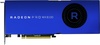
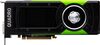
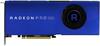
AMD Radeon PRO WX 8100 vs NVIDIA Quadro P4000

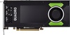
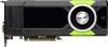
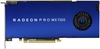
AMD Radeon PRO WX 8100
$1,199

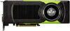
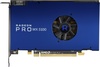
NVIDIA Quadro P4000
$815
|
3584 Shaders
16GB HBM2
1500MHz
|
1792 Shaders
8GB GDDR5
1480MHz
|
|
Peak AI Performance
21.5 TFLOPS
FP16
|
Peak AI Performance
21.22 TOPS
INT8
|
|
FP32
10.75 TFLOPS
|
FP32
5.3 TFLOPS
|
|
FP16
21.5 TFLOPS
|
FP16
80 GFLOPS
|
|
Form Factor
PCIe Card
2.0-Slots
|
Form Factor
PCIe Card
1.0-Slots
|
|
TDP
230W
|
TDP
105W
|
|
Power Connectors
1x 6-Pin
1x 8-Pin
-
-
|
Power Connectors
1x 6-Pin
-
-
-
|
|
GB6 OpenCL N/A
0%
|
GB6 OpenCL N/A
0%
|
|
GB6 Metal N/A
0%
|
GB6 Metal N/A
0%
|
|
GB6 Vulkan N/A
0%
|
GB6 Vulkan N/A
0%
|
|
GB5 OpenCL N/A
0%
|
GB5 OpenCL N/A
0%
|
|
GB5 CUDA N/A
0%
|
GB5 CUDA N/A
0%
|
|
GB5 Metal N/A
0%
|
GB5 Metal N/A
0%
|
|
GB5 Vulkan N/A
0%
|
GB5 Vulkan N/A
0%
|
|
OCT 2020.1 N/A
0%
|
OCT 2020.1 N/A
0%
|
|
OCT Metal N/A
0%
|
OCT Metal N/A
0%
|
|
Peak AI
Performance
21.5 TFLOPS
FP16
|
Peak AI
Performance
21.22 TOPS
INT8
|
|
-
-
-
|
-
-
-
|
|
-
-
-
-
-
-
|
-
-
-
-
-
-
|
|
FP16
21.5 TFLOPS
-
-
-
-
|
FP16
80 GFLOPS
-
-
-
-
|
|
FP32
10.75 TFLOPS
-
-
|
FP32
5.3 TFLOPS
-
-
|
|
FP64
670 GFLOPS
-
|
FP64
170 GFLOPS
-
|
|
-
-
-
-
|
-
-
-
-
|
|
-
-
-
|
-
-
-
|
|
-
-
-
|
-
-
-
|
|
-
-
-
-
|
INT8
21.22 TOPS
-
-
|
|
-
-
|
-
-
|
|
-
-
|
-
-
|
|
Pixel
Fillrate
96 GPixel/s
|
Pixel
Fillrate
94.72 GPixel/s
|
|
-
-
|
-
-
|
|
Texture
Fillrate
336 GTexel/s
|
Texture
Fillrate
165.76 GTexel/s
|
|
Manufacturer
AMD
|
Manufacturer
NVIDIA
|
|
Chip Designer
AMD
|
Chip Designer
NVIDIA
|
|
Architecture
GCN 5
|
Architecture
Pascal
|
|
Family
Radeon PRO WX
|
Family
Quadro P
|
|
Codename
Greenland
Vega 10
Variant
Vega 10 XL GL
|
Codename
NV134
GP104
Variant
GP104-850-A1
|
|
Market Segment
Workstation
|
Market Segment
Workstation
|
|
Release Date
9/13/2017
|
Release Date
2/6/2017
|
|
Foundry
GlobalFoundries
-
|
Foundry
TSMC
-
|
|
Fabrication Node
14LPP
-
|
Fabrication Node
16FF
-
|
|
Die Size
486 mm²
-
|
Die Size
314 mm²
-
|
|
Transistor Count
12.5 Billion
-
|
Transistor Count
7.2 Billion
-
|
|
Transistor Density
25.72M/mm²
-
|
Transistor Density
22.93M/mm²
-
|
|
Form
PCIe Card
|
Form
PCIe Card
|
|
Shading Units
3584 Shaders
-
|
Shading Units
1792 Shaders
-
|
|
Texture Mapping Units
224 TMUs
|
Texture Mapping Units
112 TMUs
|
|
Render Output Units
64 ROPs
|
Render Output Units
64 ROPs
|
|
-
-
|
-
-
|
|
-
-
|
-
-
|
|
-
-
|
Streaming Multiprocessors
14 SMs
|
|
Compute Units
56 CUs
|
-
-
|
|
-
-
|
-
-
|
|
-
-
|
-
-
|
|
-
-
1200MHz Base
1500MHz
|
-
-
1202MHz Base
1480MHz
|
|
-
-
|
-
-
|
|
L1
-
-
16KB/CU
-
|
L1
-
48KB/SM
-
-
|
|
L2
4MB Shared
|
L2
2MB Shared
|
|
-
-
-
|
-
-
-
|
|
16GB
HBM2
-
|
8GB
GDDR5
-
|
|
Bus Width
2048Bit
|
Bus Width
256Bit
|
|
Clock
945MHz
Transfer Rate
1.9GT/s
Bandwidth
483.8GB/s
|
Clock
1901MHz
Transfer Rate
7.6GT/s
Bandwidth
243.3GB/s
|
|
-
-
-
-
-
-
-
-
-
|
-
-
-
-
-
-
-
-
-
|
|
TDP
230W
|
TDP
105W
|
|
-
-
|
-
-
|
|
-
-
-
-
-
-
-
-
-
-
-
-
-
-
-
-
-
6x mini-DisplayPort 1.4
-
-
-
-
-
-
-
-
-
-
-
-
-
-
-
-
-
-
-
-
-
|
-
-
-
-
-
-
-
-
-
-
-
-
-
-
-
-
-
-
-
-
-
-
-
-
4x DisplayPort 1.4
-
-
-
-
-
-
-
-
-
-
-
-
-
-
|
|
Max Resolution
7680x4320
|
Max Resolution
7680x4320
|
|
Max Resolution Refresh Rate
60Hz
|
Max Resolution Refresh Rate
30Hz
|
|
Variable Refresh Rate
-
FreeSync
-
|
Variable Refresh Rate
G-Sync
FreeSync
-
|
|
Display Stream Compression (DSC)
Not Supported
|
Display Stream Compression (DSC)
Not Supported
|
|
Multi Monitor Support
3
|
Multi Monitor Support
3
|
|
Content Protection
HDCP 2.2
|
-
-
|
|
Model
VCE 4.0
|
Model
2x NVENC 4
|
|
Codec
-
-
-
-
-
-
-
-
AVC (H.264)
HEVC (H.265)
-
-
-
-
|
Codec
-
-
-
-
-
-
-
-
AVC (H.264)
HEVC (H.265)
-
-
-
-
|
|
Model
UVD 7.0
|
Model
NVDEC 3
|
|
Codec
MPEG-1
MPEG-2
MPEG-4
JPEG
VC-1
-
-
-
AVC (H.264)
HEVC (H.265)
-
-
-
-
|
Codec
MPEG-1
MPEG-2
MPEG-4
-
VC-1
-
VP9
-
AVC (H.264)
HEVC (H.265)
-
-
-
-
|
|
Direct X
12
Direct 3D
12_1
|
Direct X
12
Direct 3D
12_1
|
|
OpenGL
4.6
OpenCL
2.1
Vulkan
1.3
|
OpenGL
4.6
OpenCL
3.0
Vulkan
1.3
|
|
Shader Model
6.7
-
-
GFX
9
-
-
-
-
|
Shader Model
6.7
CUDA
6.1
-
-
PureVideo HD
VP8
VDPAU
Feature Set H
|
|
-
-
-
1x Fan
|
-
-
-
1x Fan
|
|
Power Connectors
-
-
1x 6-Pin
1x 8-Pin
-
-
-
|
Power Connectors
-
-
1x 6-Pin
-
-
-
-
|
|
Slots Required
2.0
PCIe Version
3.0
PCIe Lanes
16
|
Slots Required
1.0
PCIe Version
3.0
PCIe Lanes
16
|
|
Multi GPU Support
Supported
Type
CrossFire XDMA
|
Multi GPU Support
Supported
Type
4-way SLI - 2-way SLI HB
|
|
Height
111 mm (4.37 in)
Width
275 mm (10.83 in)
Depth
37 mm (1.46 in)
|
Height
111 mm (4.37 in)
Width
241 mm (9.49 in)
Depth
20 mm (0.79 in)
|


Copy Link