AMD Radeon R7 450 vs AMD Radeon Pro Duo
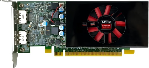
AMD Radeon R7 450

AMD Radeon Pro Duo
$1,499
|
512 Shaders
2GB GDDR5
1050MHz
|
2x 4096 Shaders
8GB (2x 4GB) HBM
1000MHz
|
|
Peak AI Performance
1.08 TFLOPS
FP32
|
Peak AI Performance
16.38 TFLOPS
FP32
|
|
FP32
1.08 TFLOPS
|
FP32
16.38 TFLOPS
|
|
-
-
|
-
-
|
|
Form Factor
PCIe Card
-
|
Form Factor
PCIe Card
2.0-Slots
|
|
TDP
65W
|
TDP
350W
|
|
Power Connectors
1x 6-Pin
-
-
-
|
Power Connectors
-
3x 8-Pin
-
-
|
|
GB6 OpenCL N/A
0%
|
|
|
GB6 Metal N/A
0%
|
GB6 Metal N/A
0%
|
|
GB6 Vulkan N/A
0%
|
|
GB5 OpenCL N/A
0%
|
GB5 OpenCL N/A
0%
|
|
GB5 CUDA N/A
0%
|
GB5 CUDA N/A
0%
|
|
GB5 Metal N/A
0%
|
GB5 Metal N/A
0%
|
|
GB5 Vulkan N/A
0%
|
GB5 Vulkan N/A
0%
|
|
OCT 2020.1 N/A
0%
|
OCT 2020.1 N/A
0%
|
|
OCT Metal N/A
0%
|
OCT Metal N/A
0%
|
|
Peak AI
Performance
1.08 TFLOPS
FP32
|
Peak AI
Performance
16.38 TFLOPS
FP32
|
|
-
-
-
|
-
-
-
|
|
-
-
-
-
-
-
|
-
-
-
-
-
-
|
|
-
-
-
-
-
-
|
-
-
-
-
-
-
|
|
FP32
1.08 TFLOPS
-
-
|
FP32
16.38 TFLOPS
-
-
|
|
FP64
70 GFLOPS
-
|
FP64
1.02 TFLOPS
-
|
|
-
-
-
-
|
-
-
-
-
|
|
-
-
-
|
-
-
-
|
|
-
-
-
|
-
-
-
|
|
-
-
-
-
|
-
-
-
-
|
|
-
-
|
-
-
|
|
-
-
|
-
-
|
|
Pixel
Fillrate
16.8 GPixel/s
|
Pixel
Fillrate
64 GPixel/s
|
|
-
-
|
-
-
|
|
Texture
Fillrate
33.6 GTexel/s
|
Texture
Fillrate
256 GTexel/s
|
|
Manufacturer
AMD
|
Manufacturer
AMD
|
|
Chip Designer
AMD
|
Chip Designer
AMD
|
|
Architecture
GCN 1
|
Architecture
GCN 3
|
|
Family
Radeon R 400
|
Family
Radeon R 300
|
|
Codename
Cape Verde
-
Variant
Cape Verde Pro
|
Codename
Fiji
-
Variant
Capsaicin XT
|
|
Market Segment
Desktop
|
Market Segment
Desktop
|
|
Release Date
6/30/2016
|
Release Date
4/26/2016
|
|
Foundry
TSMC
-
|
Foundry
TSMC
-
|
|
Fabrication Node
28nm
-
|
Fabrication Node
28nm
-
|
|
Die Size
123 mm²
-
|
Die Size
2x 596 mm²
-
|
|
Transistor Count
1.5 Billion
-
|
Transistor Count
2x 8.9 Billion
-
|
|
Transistor Density
12.20M/mm²
-
|
Transistor Density
14.93M/mm²
-
|
|
Form
PCIe Card
|
Form
PCIe Card
|
|
Shading Units
512 Shaders
-
|
Shading Units
2x 4096 Shaders
-
|
|
Texture Mapping Units
32 TMUs
|
Texture Mapping Units
2x 256 TMUs
|
|
Render Output Units
16 ROPs
|
Render Output Units
2x 64 ROPs
|
|
-
-
|
-
-
|
|
-
-
|
-
-
|
|
-
-
|
-
-
|
|
Compute Units
8 CUs
|
Compute Units
2x 64 CUs
|
|
-
-
|
-
-
|
|
-
-
|
-
-
|
|
-
-
-
1050MHz
|
-
-
-
1000MHz
|
|
-
-
|
-
-
|
|
L1
-
-
16KB/CU
-
|
L1
-
-
16KB/CU
-
|
|
L2
256KB Shared
|
L2
2MB Shared
|
|
-
-
-
|
-
-
-
|
|
2GB
GDDR5
-
|
8GB (2x 4GB)
HBM
-
|
|
Bus Width
128Bit
|
Bus Width
4096Bit
|
|
Clock
1125MHz
Transfer Rate
4.5GT/s
Bandwidth
72GB/s
|
Clock
500MHz
Transfer Rate
1GT/s
Bandwidth
512GB/s
|
|
-
-
-
-
-
-
-
-
-
|
-
-
-
-
-
-
-
-
-
|
|
TDP
65W
|
TDP
350W
|
|
-
-
|
-
-
|
|
-
-
-
-
-
-
-
-
-
-
-
-
-
-
-
-
-
-
-
-
-
-
2x DisplayPort 1.2
-
-
-
-
-
-
-
-
-
-
-
-
-
-
-
-
|
-
-
-
-
-
-
-
-
-
-
-
-
-
-
-
-
-
-
-
-
-
-
3x DisplayPort 1.2
-
-
-
-
-
-
-
-
-
-
-
1x HDMI 1.4
-
-
-
-
|
|
Max Resolution
4096x2160
|
Max Resolution
4096x2160
|
|
Max Resolution Refresh Rate
60Hz
|
Max Resolution Refresh Rate
60Hz
|
|
Variable Refresh Rate
-
-
-
|
Variable Refresh Rate
-
FreeSync
-
|
|
Display Stream Compression (DSC)
Not Supported
|
Display Stream Compression (DSC)
Not Supported
|
|
Multi Monitor Support
3
|
Multi Monitor Support
4
|
|
-
-
|
Content Protection
HDCP 1.4
|
|
Model
VCE 1.0
|
Model
VCE 3.0
|
|
Codec
-
-
-
-
-
-
-
-
AVC (H.264)
-
-
-
-
-
|
Codec
-
-
-
-
-
-
-
-
AVC (H.264)
HEVC (H.265)
-
-
-
-
|
|
Model
UVD 4.0
|
Model
UVD 6.0
|
|
Codec
MPEG-1
MPEG-2
MPEG-4
-
VC-1
-
-
-
AVC (H.264)
-
-
-
-
-
|
Codec
MPEG-1
MPEG-2
MPEG-4
JPEG
VC-1
-
-
-
AVC (H.264)
HEVC (H.265)
-
-
-
-
|
|
Direct X
12
Direct 3D
11_1
|
Direct X
12
Direct 3D
12_0
|
|
OpenGL
4.6
OpenCL
2.1
Vulkan
1.2
|
OpenGL
4.6
OpenCL
2.1
Vulkan
1.2
|
|
Shader Model
6.5
-
-
GFX
6
-
-
-
-
|
Shader Model
6.5
-
-
GFX
8
-
-
-
-
|
|
-
-
-
1x Fan
|
-
-
-
1x Fan
|
|
Power Connectors
-
-
1x 6-Pin
-
-
-
-
|
Power Connectors
-
-
-
3x 8-Pin
-
-
-
|
|
-
-
PCIe Version
3.0
PCIe Lanes
16
|
Slots Required
2.0
PCIe Version
3.0
PCIe Lanes
16
|
|
-
-
-
-
|
Multi GPU Support
Supported
Type
CrossFire XDMA
|
|
-
-
-
-
-
-
|
Height
111 mm (4.37 in)
Width
277 mm (10.91 in)
Depth
40 mm (1.57 in)
|


Copy Link