AMD Radeon RX 560 vs AMD Radeon R5 340
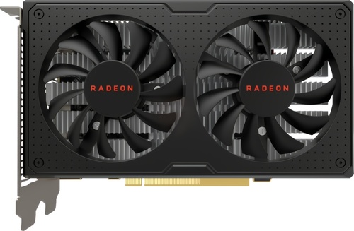
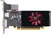
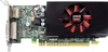
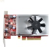
AMD Radeon RX 560
$99
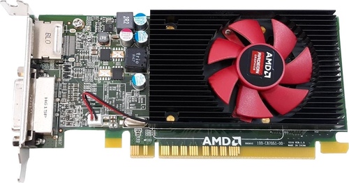
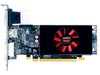
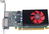
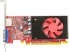
AMD Radeon R5 340
|
1024 Shaders
4GB GDDR5
1275MHz
|
384 Shaders
1GB GDDR5
825MHz
|
|
Peak AI Performance
2.61 TFLOPS
FP16
|
Peak AI Performance
630 GFLOPS
FP32
|
|
FP32
2.61 TFLOPS
|
FP32
630 GFLOPS
|
|
FP16
2.61 TFLOPS
|
-
-
|
|
Form Factor
PCIe Card
2.0-Slots
|
Form Factor
PCIe Card
1.0-Slots
|
|
TDP
75W
|
TDP
75W
|
|
-
-
-
-
-
|
-
-
-
-
-
|
|
GB6 Metal N/A
0%
|
|
|
GB5 OpenCL N/A
0%
|
GB5 OpenCL N/A
0%
|
|
GB5 CUDA N/A
0%
|
GB5 CUDA N/A
0%
|
|
GB5 Metal N/A
0%
|
GB5 Metal N/A
0%
|
|
GB5 Vulkan N/A
0%
|
GB5 Vulkan N/A
0%
|
|
OCT 2020.1 N/A
0%
|
OCT 2020.1 N/A
0%
|
|
OCT Metal N/A
0%
|
OCT Metal N/A
0%
|
|
Manufacturer
AMD
|
Manufacturer
AMD
|
|
Chip Designer
AMD
|
Chip Designer
AMD
|
|
Architecture
GCN 4
|
Architecture
GCN 1
|
|
Family
Radeon RX 500
|
Family
Radeon R 300
|
|
Codename
Baffin
Polaris 21
Variant
Polaris 21 XT
|
Codename
Oland
-
Variant
Oland XT
|
|
Market Segment
Desktop
|
Market Segment
Desktop
|
|
Release Date
4/18/2017
|
Release Date
5/5/2015
|
|
Foundry
GlobalFoundries
-
|
Foundry
TSMC
-
|
|
Fabrication Node
14LPP
-
|
Fabrication Node
28nm
-
|
|
Die Size
123 mm²
-
|
Die Size
90 mm²
-
|
|
Transistor Count
3 Billion
-
|
Transistor Count
1 Billion
-
|
|
Transistor Density
24.39M/mm²
-
|
Transistor Density
11.56M/mm²
-
|
|
Form
PCIe Card
|
Form
PCIe Card
|
|
Shading Units
1024 Shaders
-
|
Shading Units
384 Shaders
-
|
|
Texture Mapping Units
64 TMUs
|
Texture Mapping Units
24 TMUs
|
|
Render Output Units
16 ROPs
|
Render Output Units
8 ROPs
|
|
-
-
|
-
-
|
|
-
-
|
-
-
|
|
-
-
|
-
-
|
|
Compute Units
16 CUs
|
Compute Units
6 CUs
|
|
-
-
|
-
-
|
|
-
-
|
-
-
|
|
-
-
1175MHz Base
1275MHz
|
-
-
-
825MHz
|
|
Peak AI Performance
2.61 TFLOPS
FP16
|
Peak AI Performance
630 GFLOPS
FP32
|
|
-
-
-
|
-
-
-
|
|
-
-
-
-
-
-
|
-
-
-
-
-
-
|
|
FP16
2.61 TFLOPS
-
-
-
-
|
-
-
-
-
-
-
|
|
FP32
2.61 TFLOPS
-
-
|
FP32
630 GFLOPS
-
-
|
|
FP64
160 GFLOPS
-
|
FP64
40 GFLOPS
-
|
|
-
-
-
-
|
-
-
-
-
|
|
-
-
-
|
-
-
-
|
|
-
-
-
|
-
-
-
|
|
-
-
-
-
|
-
-
-
-
|
|
-
-
|
-
-
|
|
-
-
|
-
-
|
|
Pixel Fillrate
20.4 GPixel/s
|
Pixel Fillrate
6.6 GPixel/s
|
|
-
-
|
-
-
|
|
Texture Fillrate
81.6 GTexel/s
|
Texture Fillrate
19.8 GTexel/s
|
|
-
-
|
-
-
|
|
L1
-
-
16KB/CU
-
|
L1
-
-
16KB/CU
-
|
|
L2
1MB Shared
|
L2
256KB Shared
|
|
-
-
-
|
-
-
-
|
|
4GB
GDDR5
-
|
1GB
GDDR5
-
|
|
Bus Width
128Bit
|
Bus Width
128Bit
|
|
Clock
1750MHz
Transfer Rate
7GT/s
Bandwidth
112GB/s
|
Clock
1125MHz
Transfer Rate
4.5GT/s
Bandwidth
72GB/s
|
|
-
-
-
-
-
-
-
-
-
|
-
-
-
-
-
-
-
-
-
|
|
TDP
75W
|
TDP
75W
|
|
-
-
|
-
-
|
|
-
-
-
-
-
-
-
-
-
-
1x DVI-D Dual-Link
-
-
-
-
-
-
-
-
-
-
-
-
-
1x DisplayPort 1.4
-
-
-
-
-
-
-
-
-
-
1x HDMI 2.0
-
-
-
|
-
-
-
-
-
-
-
-
1x DVI-I Dual-Link
-
-
-
-
-
-
-
-
-
-
-
-
-
1x DisplayPort 1.2
-
-
-
-
-
-
-
-
-
-
-
-
-
-
-
-
|
|
Max Resolution
5120x2880
|
Max Resolution
4096x2160
|
|
Max Resolution Refresh Rate
60Hz
|
Max Resolution Refresh Rate
60Hz
|
|
Variable Refresh Rate
-
FreeSync
-
|
Variable Refresh Rate
-
-
-
|
|
Display Stream Compression (DSC)
Not Supported
|
Display Stream Compression (DSC)
Not Supported
|
|
Multi Monitor Support
3
|
Multi Monitor Support
3
|
|
Content Protection
HDCP 2.2
|
-
-
|
|
Model
VCE 3.4
|
Model
VCE 1.0
|
|
Codec
-
-
-
-
-
-
-
-
AVC (H.264)
HEVC (H.265)
-
-
-
-
|
Codec
-
-
-
-
-
-
-
-
AVC (H.264)
-
-
-
-
-
|
|
Model
UVD 6.3
|
Model
UVD 4.0
|
|
Codec
MPEG-1
MPEG-2
MPEG-4
JPEG
VC-1
-
-
-
AVC (H.264)
HEVC (H.265)
-
-
-
-
|
Codec
MPEG-1
MPEG-2
MPEG-4
-
VC-1
-
-
-
AVC (H.264)
-
-
-
-
-
|
|
Direct X
12
Direct 3D
12_0
|
Direct X
12
Direct 3D
11_1
|
|
OpenGL
4.6
OpenCL
2.1
Vulkan
1.3
|
OpenGL
4.6
OpenCL
2.1
Vulkan
1.2
|
|
Shader Model
6.7
-
-
GFX
8
-
-
-
-
|
Shader Model
6.5
-
-
GFX
6
-
-
-
-
|
|
-
-
-
2x Fans
|
-
-
-
1x Fan
|
|
-
-
-
-
-
-
-
-
|
-
-
-
-
-
-
-
-
|
|
Slots Required
2.0
PCIe Version
3.0
PCIe Lanes
8
|
Slots Required
1.0
PCIe Version
3.0
PCIe Lanes
16
|
|
Multi GPU Support
Supported
Type
CrossFire XDMA
|
-
-
-
-
|
|
Height
110 mm (4.33 in)
Width
170 mm (6.69 in)
Depth
37 mm (1.46 in)
|
-
-
-
-
-
-
|


Copy Link