AMD Radeon RX 7900 XT vs AMD Radeon R7 350X
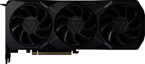
AMD Radeon RX 7900 XT
$899
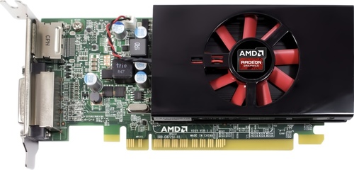
AMD Radeon R7 350X
|
5376 Shaders
20GB GDDR6
2400MHz
|
384 Shaders
4GB DDR3
1050MHz
|
|
Peak AI Performance
206.44 TOPS
INT4 Tensor
|
Peak AI Performance
810 GFLOPS
FP32
|
|
FP32
51.61 TFLOPS
|
FP32
810 GFLOPS
|
|
FP16
103.22 TFLOPS
|
-
-
|
|
Form Factor
PCIe Card
2.5-Slots
|
Form Factor
PCIe Card
1.0-Slots
|
|
TDP
315W
|
TDP
30W
|
|
Power Connectors
-
2x 8-Pin
-
-
|
-
-
-
-
-
|
|
GB6 Metal N/A
0%
|
GB6 Metal N/A
0%
|
|
GB5 OpenCL N/A
0%
|
GB5 OpenCL N/A
0%
|
|
GB5 CUDA N/A
0%
|
GB5 CUDA N/A
0%
|
|
GB5 Metal N/A
0%
|
GB5 Metal N/A
0%
|
|
GB5 Vulkan N/A
0%
|
GB5 Vulkan N/A
0%
|
|
OCT 2020.1 N/A
0%
|
OCT 2020.1 N/A
0%
|
|
OCT Metal N/A
0%
|
OCT Metal N/A
0%
|
|
Manufacturer
AMD
|
Manufacturer
AMD
|
|
Chip Designer
AMD
|
Chip Designer
AMD
|
|
Architecture
RDNA 3
|
Architecture
GCN 1
|
|
Family
Radeon RX 7000
|
Family
Radeon R 300
|
|
Codename
Plum Bonito
Navi 31
Variant
Navi 31 XT
|
Codename
Oland
-
Variant
Oland XT
|
|
Market Segment
Desktop
|
Market Segment
Desktop
|
|
Release Date
12/13/2022
|
Release Date
5/5/2015
|
|
Foundry
TSMC
TSMC Memory Cache Die
|
Foundry
TSMC
-
|
|
Fabrication Node
N5
N6 Memory Cache Die
|
Fabrication Node
28nm
-
|
|
Die Size
304 mm²
6x 38 mm² Memory Cache Die
|
Die Size
90 mm²
-
|
|
Transistor Count
45.4 Billion
6x 2.1 Billion Memory Cache Die
|
Transistor Count
1 Billion
-
|
|
Transistor Density
149.17M/mm²
54.64M/mm² Memory Cache Die
|
Transistor Density
11.56M/mm²
-
|
|
Form
PCIe Card
|
Form
PCIe Card
|
|
Shading Units
5376 Shaders
-
|
Shading Units
384 Shaders
-
|
|
Texture Mapping Units
336 TMUs
|
Texture Mapping Units
24 TMUs
|
|
Render Output Units
192 ROPs
|
Render Output Units
8 ROPs
|
|
Tensor Cores
168 T-Cores
|
-
-
|
|
Ray-Tracing Cores
84 RT-Cores
|
-
-
|
|
-
-
|
-
-
|
|
Compute Units
84 CUs
|
Compute Units
6 CUs
|
|
-
-
|
-
-
|
|
-
-
|
-
-
|
|
-
-
1500MHz Base
2400MHz
|
-
-
-
1050MHz
|
|
Peak AI Performance
206.44 TOPS
INT4 Tensor
|
Peak AI Performance
810 GFLOPS
FP32
|
|
-
-
-
|
-
-
-
|
|
-
-
-
-
-
-
|
-
-
-
-
-
-
|
|
FP16
103.22 TFLOPS
51.61 TFLOPS Tensor (FP16 Accumulate)
-
51.61 TFLOPS Tensor (FP32 Accumulate)
-
|
-
-
-
-
-
-
|
|
FP32
51.61 TFLOPS
-
-
|
FP32
810 GFLOPS
-
-
|
|
FP64
1.61 TFLOPS
-
|
FP64
50 GFLOPS
-
|
|
BF16
103.22 TFLOPS
51.61 TFLOPS Tensor
-
|
-
-
-
-
|
|
-
-
-
|
-
-
-
|
|
INT4
206.44 TOPS Tensor
-
|
-
-
-
|
|
INT8
-
51.61 TOPS Tensor
-
|
-
-
-
-
|
|
INT32
25.8 TOPS
|
-
-
|
|
-
-
|
-
-
|
|
Pixel Fillrate
460.8 GPixel/s
|
Pixel Fillrate
8.4 GPixel/s
|
|
-
-
|
-
-
|
|
Texture Fillrate
806.4 GTexel/s
|
Texture Fillrate
25.2 GTexel/s
|
|
L0
64KB/WGP
|
-
-
|
|
L1
-
-
-
256KB/Array
|
L1
-
-
16KB/CU
-
|
|
L2
6MB Shared
|
L2
256KB Shared
|
|
L3
80MB Shared
2.9TB/s
|
-
-
-
|
|
20GB
GDDR6
-
|
4GB
DDR3
-
|
|
Bus Width
320Bit
|
Bus Width
128Bit
|
|
Clock
2500MHz
Transfer Rate
20GT/s
Bandwidth
800GB/s
|
Clock
500MHz
Transfer Rate
1GT/s
Bandwidth
16GB/s
|
|
-
-
-
-
-
-
-
-
-
|
-
-
-
-
-
-
-
-
-
|
|
TDP
315W
|
TDP
30W
|
|
-
-
|
-
-
|
|
-
-
-
-
-
-
-
-
-
-
-
-
-
-
-
-
-
-
-
-
-
-
-
-
-
-
2x DisplayPort 2.1
-
-
-
-
-
-
-
-
-
1x HDMI 2.1
1x USB-C + DP
-
|
-
-
-
-
-
-
-
-
1x DVI-I Dual-Link
-
-
-
-
-
-
-
-
-
-
-
-
-
1x DisplayPort 1.2
-
-
-
-
-
-
-
-
-
-
-
-
-
-
-
-
|
|
Max Resolution
15360x8640
|
Max Resolution
4096x2160
|
|
Max Resolution Refresh Rate
165Hz
|
Max Resolution Refresh Rate
60Hz
|
|
Variable Refresh Rate
-
FreeSync
-
|
Variable Refresh Rate
-
-
-
|
|
Display Stream Compression (DSC)
Supported
|
Display Stream Compression (DSC)
Not Supported
|
|
Multi Monitor Support
3
|
Multi Monitor Support
3
|
|
Content Protection
HDCP 2.3
|
-
-
|
|
Model
VCN 4.0
|
Model
VCE 1.0
|
|
Codec
-
-
-
-
-
-
VP9
-
AVC (H.264)
HEVC (H.265)
-
AV1
-
-
|
Codec
-
-
-
-
-
-
-
-
AVC (H.264)
-
-
-
-
-
|
|
Model
VCN 4.0
|
Model
UVD 4.0
|
|
Codec
MPEG-1
MPEG-2
MPEG-4
JPEG
VC-1
-
VP9
-
AVC (H.264)
HEVC (H.265)
-
AV1
-
-
|
Codec
MPEG-1
MPEG-2
MPEG-4
-
VC-1
-
-
-
AVC (H.264)
-
-
-
-
-
|
|
Direct X
12
Direct 3D
12_2
|
Direct X
12
Direct 3D
11_1
|
|
OpenGL
4.6
OpenCL
2.2
Vulkan
1.3
|
OpenGL
4.6
OpenCL
2.1
Vulkan
1.2
|
|
Shader Model
6.7
-
-
GFX
11
-
-
-
-
|
Shader Model
6.5
-
-
GFX
6
-
-
-
-
|
|
-
-
-
3x Fans
|
-
-
-
1x Fan
|
|
Power Connectors
-
-
-
2x 8-Pin
-
-
-
|
-
-
-
-
-
-
-
-
|
|
Slots Required
2.5
PCIe Version
4.0
PCIe Lanes
16
|
Slots Required
1.0
PCIe Version
3.0
PCIe Lanes
16
|
|
Multi GPU Support
Supported
Type
CrossFire XDMA
|
-
-
-
-
|
|
Height
110 mm (4.33 in)
Width
276 mm (10.87 in)
Depth
51 mm (2.01 in)
|
-
-
-
-
-
-
|


Copy Link