AMD Radeon VII vs AMD Radeon R7 435
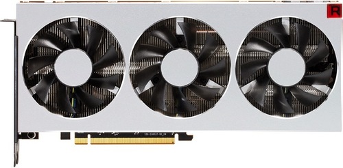
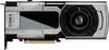
AMD Radeon VII
$699

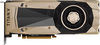
AMD Radeon R7 435
|
3840 Shaders
16GB HBM2
1800MHz
|
320 Shaders
2GB DDR3
920MHz
|
|
Peak AI Performance
27.65 TFLOPS
FP16
|
Peak AI Performance
590 GFLOPS
FP32
|
|
FP32
13.82 TFLOPS
|
FP32
590 GFLOPS
|
|
FP16
27.65 TFLOPS
|
-
-
|
|
Form Factor
PCIe Card
2.0-Slots
|
Form Factor
PCIe Card
1.0-Slots
|
|
TDP
300W
|
TDP
50W
|
|
Power Connectors
-
2x 8-Pin
-
-
|
-
-
-
-
-
|
|
GB6 OpenCL N/A
0%
|
|
|
GB6 Metal 74,340
30%
|
GB6 Metal N/A
0%
|
|
GB6 Vulkan N/A
0%
|
|
GB5 OpenCL N/A
0%
|
GB5 OpenCL N/A
0%
|
|
GB5 CUDA N/A
0%
|
GB5 CUDA N/A
0%
|
|
GB5 Metal N/A
0%
|
GB5 Metal N/A
0%
|
|
GB5 Vulkan N/A
0%
|
GB5 Vulkan N/A
0%
|
|
OCT 2020.1 N/A
0%
|
OCT 2020.1 N/A
0%
|
|
OCT Metal N/A
0%
|
OCT Metal N/A
0%
|
|
Peak AI
Performance
27.65 TFLOPS
FP16
|
Peak AI
Performance
590 GFLOPS
FP32
|
|
-
-
-
|
-
-
-
|
|
-
-
-
-
-
-
|
-
-
-
-
-
-
|
|
FP16
27.65 TFLOPS
-
-
-
-
|
-
-
-
-
-
-
|
|
FP32
13.82 TFLOPS
-
-
|
FP32
590 GFLOPS
-
-
|
|
FP64
3.46 TFLOPS
-
|
FP64
40 GFLOPS
-
|
|
-
-
-
-
|
-
-
-
-
|
|
-
-
-
|
-
-
-
|
|
-
-
-
|
-
-
-
|
|
-
-
-
-
|
-
-
-
-
|
|
-
-
|
-
-
|
|
-
-
|
-
-
|
|
Pixel
Fillrate
115.2 GPixel/s
|
Pixel
Fillrate
7.36 GPixel/s
|
|
-
-
|
-
-
|
|
Texture
Fillrate
432 GTexel/s
|
Texture
Fillrate
18.4 GTexel/s
|
|
Manufacturer
AMD
|
Manufacturer
AMD
|
|
Chip Designer
AMD
|
Chip Designer
AMD
|
|
Architecture
GCN 5
|
Architecture
GCN 1
|
|
Family
Radeon RX Vega
|
Family
Radeon R 400
|
|
Codename
Moonshot
Vega 20
Variant
Vega 20 XT
|
Codename
Oland
-
Variant
Oland Pro
|
|
Market Segment
Desktop
|
Market Segment
Desktop
|
|
Release Date
2/7/2019
|
Release Date
6/30/2016
|
|
Foundry
TSMC
-
|
Foundry
TSMC
-
|
|
Fabrication Node
N7
-
|
Fabrication Node
28nm
-
|
|
Die Size
331 mm²
-
|
Die Size
90 mm²
-
|
|
Transistor Count
13.2 Billion
-
|
Transistor Count
1 Billion
-
|
|
Transistor Density
39.97M/mm²
-
|
Transistor Density
11.56M/mm²
-
|
|
Form
PCIe Card
|
Form
PCIe Card
|
|
Shading Units
3840 Shaders
-
|
Shading Units
320 Shaders
-
|
|
Texture Mapping Units
240 TMUs
|
Texture Mapping Units
20 TMUs
|
|
Render Output Units
64 ROPs
|
Render Output Units
8 ROPs
|
|
-
-
|
-
-
|
|
-
-
|
-
-
|
|
-
-
|
-
-
|
|
Compute Units
60 CUs
|
Compute Units
5 CUs
|
|
-
-
|
-
-
|
|
-
-
|
-
-
|
|
-
-
1400MHz Base
1800MHz
|
-
-
-
920MHz
|
|
-
-
|
-
-
|
|
L1
-
-
16KB/CU
-
|
L1
-
-
16KB/CU
-
|
|
L2
4MB Shared
|
L2
256KB Shared
|
|
-
-
-
|
-
-
-
|
|
16GB
HBM2
-
|
2GB
DDR3
-
|
|
Bus Width
4096Bit
|
Bus Width
64Bit
|
|
Clock
1000MHz
Transfer Rate
2GT/s
Bandwidth
1024GB/s
|
Clock
1000MHz
Transfer Rate
2GT/s
Bandwidth
16GB/s
|
|
-
-
-
-
-
-
-
-
-
|
-
-
-
-
-
-
-
-
-
|
|
TDP
300W
|
TDP
50W
|
|
-
-
|
-
-
|
|
-
-
-
-
-
-
-
-
-
-
-
-
-
-
-
-
-
-
-
-
-
-
-
-
3x DisplayPort 1.4
-
-
-
-
-
-
-
-
-
-
1x HDMI 2.0
-
-
-
|
1x VGA
-
-
-
-
-
-
-
1x DVI-I Dual-Link
-
-
-
-
-
-
-
-
-
-
-
-
-
-
-
-
-
-
-
-
-
-
-
-
-
1x HDMI 1.4
-
-
-
-
|
|
Max Resolution
7680x4320
|
Max Resolution
4096x2160
|
|
Max Resolution Refresh Rate
60Hz
|
Max Resolution Refresh Rate
60Hz
|
|
Variable Refresh Rate
-
FreeSync
-
|
Variable Refresh Rate
-
-
-
|
|
Display Stream Compression (DSC)
Not Supported
|
Display Stream Compression (DSC)
Not Supported
|
|
Multi Monitor Support
3
|
Multi Monitor Support
3
|
|
Content Protection
HDCP 2.2
|
-
-
|
|
Model
VCE 4.1
|
Model
VCE 1.0
|
|
Codec
-
-
-
-
-
-
-
-
AVC (H.264)
HEVC (H.265)
-
-
-
-
|
Codec
-
-
-
-
-
-
-
-
AVC (H.264)
-
-
-
-
-
|
|
Model
UVD 7.2
|
Model
UVD 4.0
|
|
Codec
MPEG-1
MPEG-2
MPEG-4
JPEG
VC-1
-
-
-
AVC (H.264)
HEVC (H.265)
-
-
-
-
|
Codec
MPEG-1
MPEG-2
MPEG-4
-
VC-1
-
-
-
AVC (H.264)
-
-
-
-
-
|
|
Direct X
12
Direct 3D
12_1
|
Direct X
12
Direct 3D
11_1
|
|
OpenGL
4.6
OpenCL
2.1
Vulkan
1.3
|
OpenGL
4.6
OpenCL
2.1
Vulkan
1.2
|
|
Shader Model
6.7
-
-
GFX
9
-
-
-
-
|
Shader Model
6.5
-
-
GFX
6
-
-
-
-
|
|
-
-
-
3x Fans
|
-
-
-
1x Fan
|
|
Power Connectors
-
-
-
2x 8-Pin
-
-
-
|
-
-
-
-
-
-
-
-
|
|
Slots Required
2.0
PCIe Version
3.0
PCIe Lanes
16
|
Slots Required
1.0
PCIe Version
3.0
PCIe Lanes
8
|
|
Multi GPU Support
Supported
Type
CrossFire XDMA
|
-
-
-
-
|
|
Height
125 mm (4.92 in)
Width
280 mm (11.02 in)
Depth
40 mm (1.57 in)
|
-
-
-
-
-
-
|


Copy Link