Radeon Pro Vega II Duo vs NVIDIA Quadro P6000
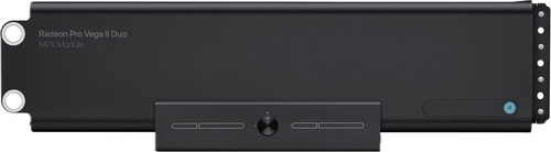
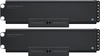
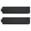
Radeon Pro Vega II Duo
$5,600

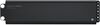
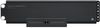
NVIDIA Quadro P6000
$5,999
|
2x 4096 Shaders
64GB (2x 32GB) HBM2
1720MHz
|
3840 Shaders
24GB GDDR5X
1645MHz
|
|
Peak AI Performance
56.36 TFLOPS
FP16
|
Peak AI Performance
50.53 TOPS
INT8
|
|
FP32
28.18 TFLOPS
|
FP32
12.63 TFLOPS
|
|
FP16
56.36 TFLOPS
|
FP16
200 GFLOPS
|
|
Form Factor
MPX
4.0-Slots
|
Form Factor
PCIe Card
2.0-Slots
|
|
TDP
475W
|
TDP
250W
|
|
-
-
-
-
-
|
Power Connectors
-
1x 8-Pin
-
-
|
|
GB6 OpenCL N/A
0%
|
|
|
GB6 Metal N/A
0%
|
|
|
GB6 Vulkan N/A
0%
|
GB6 Vulkan N/A
0%
|
|
GB5 OpenCL N/A
0%
|
GB5 OpenCL N/A
0%
|
|
GB5 CUDA N/A
0%
|
GB5 CUDA N/A
0%
|
|
GB5 Metal N/A
0%
|
GB5 Metal N/A
0%
|
|
GB5 Vulkan N/A
0%
|
GB5 Vulkan N/A
0%
|
|
OCT 2020.1 N/A
0%
|
OCT 2020.1 N/A
0%
|
|
OCT Metal N/A
0%
|
OCT Metal N/A
0%
|
|
Peak AI
Performance
56.36 TFLOPS
FP16
|
Peak AI
Performance
50.53 TOPS
INT8
|
|
-
-
-
|
-
-
-
|
|
-
-
-
-
-
-
|
-
-
-
-
-
-
|
|
FP16
56.36 TFLOPS
-
-
-
-
|
FP16
200 GFLOPS
-
-
-
-
|
|
FP32
28.18 TFLOPS
-
-
|
FP32
12.63 TFLOPS
-
-
|
|
FP64
7.05 TFLOPS
-
|
FP64
400 GFLOPS
-
|
|
-
-
-
-
|
-
-
-
-
|
|
-
-
-
|
-
-
-
|
|
-
-
-
|
-
-
-
|
|
-
-
-
-
|
INT8
50.53 TOPS
-
-
|
|
-
-
|
-
-
|
|
-
-
|
-
-
|
|
Pixel
Fillrate
110.08 GPixel/s
|
Pixel
Fillrate
157.92 GPixel/s
|
|
-
-
|
-
-
|
|
Texture
Fillrate
440.32 GTexel/s
|
Texture
Fillrate
394.8 GTexel/s
|
|
Manufacturer
Apple
|
Manufacturer
NVIDIA
|
|
Chip Designer
AMD
|
Chip Designer
NVIDIA
|
|
Architecture
GCN 5
|
Architecture
Pascal
|
|
Family
Radeon Pro Vega
|
Family
Quadro P
|
|
Codename
Moonshot
Vega 20
Variant
Vega 20 XTXA
|
Codename
NV132
GP102
Variant
GP102-875-A1
|
|
Market Segment
Workstation
|
Market Segment
Workstation
|
|
Release Date
12/1/2019
|
Release Date
10/1/2016
|
|
Foundry
TSMC
-
|
Foundry
TSMC
-
|
|
Fabrication Node
N7
-
|
Fabrication Node
16FF
-
|
|
Die Size
2x 331 mm²
-
|
Die Size
471 mm²
-
|
|
Transistor Count
2x 13.2 Billion
-
|
Transistor Count
11.8 Billion
-
|
|
Transistor Density
39.97M/mm²
-
|
Transistor Density
25.05M/mm²
-
|
|
Form
MPX
|
Form
PCIe Card
|
|
Shading Units
2x 4096 Shaders
-
|
Shading Units
3840 Shaders
-
|
|
Texture Mapping Units
2x 256 TMUs
|
Texture Mapping Units
240 TMUs
|
|
Render Output Units
2x 64 ROPs
|
Render Output Units
96 ROPs
|
|
-
-
|
-
-
|
|
-
-
|
-
-
|
|
-
-
|
Streaming Multiprocessors
30 SMs
|
|
Compute Units
2x 64 CUs
|
-
-
|
|
-
-
|
-
-
|
|
-
-
|
Graphics Processing Clusters
6 GPCs
|
|
-
-
-
1720MHz
|
-
-
1506MHz Base
1645MHz
|
|
-
-
|
-
-
|
|
L1
-
-
16KB/CU
-
|
L1
-
48KB/SM
-
-
|
|
L2
4MB Shared
|
L2
3MB Shared
|
|
-
-
-
|
-
-
-
|
|
64GB (2x 32GB)
HBM2
-
|
24GB
GDDR5X
-
|
|
Bus Width
4096Bit
|
Bus Width
384Bit
|
|
Clock
1000MHz
Transfer Rate
2GT/s
Bandwidth
1024GB/s
|
Clock
1126MHz
Transfer Rate
9GT/s
Bandwidth
432.4GB/s
|
|
-
-
-
-
-
-
-
-
-
|
-
-
-
-
-
-
-
-
-
|
|
TDP
475W
|
TDP
250W
|
|
-
-
|
-
-
|
|
-
-
-
-
-
-
-
-
-
-
-
-
-
-
-
-
-
-
-
-
-
-
-
-
-
-
-
-
-
-
-
-
-
-
-
1x HDMI 2.0
-
-
4x Thunderbolt 3 (40Gbps)
|
-
-
-
-
-
-
-
-
-
-
1x DVI-D Dual-Link
-
-
-
-
-
-
-
-
-
-
-
-
-
4x DisplayPort 1.4
-
-
-
-
-
-
-
-
-
-
-
-
-
-
|
|
Max Resolution
7680x4320
|
Max Resolution
7680x4320
|
|
Max Resolution Refresh Rate
60Hz
|
Max Resolution Refresh Rate
30Hz
|
|
Variable Refresh Rate
-
FreeSync
-
|
Variable Refresh Rate
G-Sync
FreeSync
-
|
|
Display Stream Compression (DSC)
Not Supported
|
Display Stream Compression (DSC)
Not Supported
|
|
Multi Monitor Support
3
|
Multi Monitor Support
3
|
|
Content Protection
HDCP 2.2
|
-
-
|
|
Model
VCE 4.1
|
Model
2x NVENC 4
|
|
Codec
-
-
-
-
-
-
-
-
AVC (H.264)
HEVC (H.265)
-
-
-
-
|
Codec
-
-
-
-
-
-
-
-
AVC (H.264)
HEVC (H.265)
-
-
-
-
|
|
Model
UVD 7.2
|
Model
NVDEC 3
|
|
Codec
MPEG-1
MPEG-2
MPEG-4
JPEG
VC-1
-
-
-
AVC (H.264)
HEVC (H.265)
-
-
-
-
|
Codec
MPEG-1
MPEG-2
MPEG-4
-
VC-1
-
VP9
-
AVC (H.264)
HEVC (H.265)
-
-
-
-
|
|
Direct X
12
Direct 3D
12_1
|
Direct X
12
Direct 3D
12_1
|
|
OpenGL
4.6
OpenCL
2.1
Vulkan
1.3
|
OpenGL
4.6
OpenCL
3.0
Vulkan
1.3
|
|
Shader Model
6.7
-
-
GFX
9
-
-
-
-
|
Shader Model
6.7
CUDA
6.1
-
-
PureVideo HD
VP8
VDPAU
Feature Set H
|
|
-
-
-
-
|
-
-
-
1x Fan
|
|
-
-
-
-
-
-
-
-
|
Power Connectors
-
-
-
1x 8-Pin
-
-
-
|
|
Slots Required
4.0
PCIe Version
3.0
PCIe Lanes
16
|
Slots Required
2.0
PCIe Version
3.0
PCIe Lanes
16
|
|
Multi GPU Support
Supported
Type
CrossFire XDMA
|
Multi GPU Support
Supported
Type
4-way SLI - 2-way SLI HB
|
|
-
-
-
-
-
-
|
Height
111 mm (4.37 in)
Width
267 mm (10.51 in)
Depth
40 mm (1.57 in)
|


Copy Link