Radeon Pro W6900X vs NVIDIA Quadro P1000
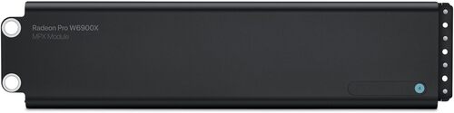
Radeon Pro W6900X
$6,000

NVIDIA Quadro P1000
|
5120 Shaders
32GB GDDR6
2171MHz
|
640 Shaders
4GB GDDR5
1481MHz
|
|
Peak AI Performance
44.46 TFLOPS
FP16
|
Peak AI Performance
7.58 TOPS
INT8
|
|
FP32
22.23 TFLOPS
|
FP32
1.9 TFLOPS
|
|
FP16
44.46 TFLOPS
|
FP16
30 GFLOPS
|
|
Form Factor
MPX
4.0-Slots
|
Form Factor
PCIe Card
1.0-Slots
|
|
TDP
300W
|
TDP
47W
|
|
-
-
-
-
-
|
-
-
-
-
-
|
|
GB6 Metal N/A
0%
|
|
|
GB6 Vulkan N/A
0%
|
|
GB5 OpenCL 120,660
40%
|
GB5 OpenCL N/A
0%
|
|
GB5 CUDA N/A
0%
|
GB5 CUDA N/A
0%
|
|
GB5 Metal 154,880
86%
|
GB5 Metal N/A
0%
|
|
GB5 Vulkan N/A
0%
|
GB5 Vulkan N/A
0%
|
|
OCT 2020.1 N/A
0%
|
OCT 2020.1 N/A
0%
|
|
OCT Metal 435
74%
|
OCT Metal N/A
0%
|
|
Peak AI
Performance
44.46 TFLOPS
FP16
|
Peak AI
Performance
7.58 TOPS
INT8
|
|
-
-
-
|
-
-
-
|
|
-
-
-
-
-
-
|
-
-
-
-
-
-
|
|
FP16
44.46 TFLOPS
-
-
-
-
|
FP16
30 GFLOPS
-
-
-
-
|
|
FP32
22.23 TFLOPS
-
-
|
FP32
1.9 TFLOPS
-
-
|
|
FP64
1.39 TFLOPS
-
|
FP64
60 GFLOPS
-
|
|
-
-
-
-
|
-
-
-
-
|
|
-
-
-
|
-
-
-
|
|
-
-
-
|
-
-
-
|
|
-
-
-
-
|
INT8
7.58 TOPS
-
-
|
|
-
-
|
-
-
|
|
-
-
|
-
-
|
|
Pixel
Fillrate
277.888 GPixel/s
|
Pixel
Fillrate
47.392 GPixel/s
|
|
-
-
|
-
-
|
|
Texture
Fillrate
694.72 GTexel/s
|
Texture
Fillrate
59.24 GTexel/s
|
|
Manufacturer
Apple
|
Manufacturer
NVIDIA
|
|
Chip Designer
AMD
|
Chip Designer
NVIDIA
|
|
Architecture
RDNA 2
|
Architecture
Pascal
|
|
Family
Radeon Pro W
|
Family
Quadro P
|
|
Codename
Sienna Cichlid
Navi 21
Variant
Navi 21 XTA
|
Codename
NV137
GP107
Variant
GP107-880-KA-A1
|
|
Market Segment
Workstation
|
Market Segment
Workstation
|
|
Release Date
8/3/2021
|
Release Date
2/7/2017
|
|
Foundry
TSMC
-
|
Foundry
Samsung
-
|
|
Fabrication Node
N7
-
|
Fabrication Node
14LPP
-
|
|
Die Size
520 mm²
-
|
Die Size
132 mm²
-
|
|
Transistor Count
26.8 Billion
-
|
Transistor Count
3.3 Billion
-
|
|
Transistor Density
51.56M/mm²
-
|
Transistor Density
25.00M/mm²
-
|
|
Form
MPX
|
Form
PCIe Card
|
|
Shading Units
5120 Shaders
-
|
Shading Units
640 Shaders
-
|
|
Texture Mapping Units
320 TMUs
|
Texture Mapping Units
40 TMUs
|
|
Render Output Units
128 ROPs
|
Render Output Units
32 ROPs
|
|
-
-
|
-
-
|
|
Ray-Tracing Cores
80 RT-Cores
|
-
-
|
|
-
-
|
Streaming Multiprocessors
5 SMs
|
|
Compute Units
80 CUs
|
-
-
|
|
-
-
|
-
-
|
|
Graphics Processing Clusters
4 GPCs
|
-
-
|
|
-
-
1825MHz Base
2171MHz
|
-
-
1266MHz Base
1481MHz
|
|
L0
32KB/WGP
|
-
-
|
|
L1
-
-
-
128KB/Array
|
L1
-
48KB/SM
-
-
|
|
L2
4MB Shared
|
L2
1MB Shared
|
|
L3
128MB Shared
1.66TB/s
|
-
-
-
|
|
32GB
GDDR6
-
|
4GB
GDDR5
-
|
|
Bus Width
256Bit
|
Bus Width
128Bit
|
|
Clock
2000MHz
Transfer Rate
16GT/s
Bandwidth
512GB/s
|
Clock
1752MHz
Transfer Rate
7GT/s
Bandwidth
112.1GB/s
|
|
-
-
-
-
-
-
-
-
-
|
-
-
-
-
-
-
-
-
-
|
|
TDP
300W
|
TDP
47W
|
|
Temp
100°C Max
|
-
-
|
|
-
-
-
-
-
-
-
-
-
-
-
-
-
-
-
-
-
-
-
-
-
-
-
-
-
-
-
-
-
-
-
-
-
-
-
1x HDMI 2.0
-
-
4x Thunderbolt 3 (40Gbps)
|
-
-
-
-
-
-
-
-
-
-
-
-
-
-
-
-
-
4x mini-DisplayPort 1.4
-
-
-
-
-
-
-
-
-
-
-
-
-
-
-
-
-
-
-
-
-
|
|
Max Resolution
6016x3384
|
Max Resolution
7680x4320
|
|
Max Resolution Refresh Rate
60Hz
|
Max Resolution Refresh Rate
30Hz
|
|
Variable Refresh Rate
-
FreeSync
-
|
Variable Refresh Rate
G-Sync
FreeSync
-
|
|
Display Stream Compression (DSC)
Supported
|
Display Stream Compression (DSC)
Not Supported
|
|
Multi Monitor Support
6
|
Multi Monitor Support
3
|
|
Content Protection
HDCP 2.3
|
-
-
|
|
Model
VCN 3.0
|
Model
NVENC 4
|
|
Codec
-
-
-
-
-
-
-
-
AVC (H.264)
HEVC (H.265)
-
-
-
-
|
Codec
-
-
-
-
-
-
-
-
AVC (H.264)
HEVC (H.265)
-
-
-
-
|
|
Model
VCN 3.0
|
Model
NVDEC 3
|
|
Codec
MPEG-1
MPEG-2
MPEG-4
JPEG
VC-1
-
VP9
-
AVC (H.264)
HEVC (H.265)
-
AV1
-
-
|
Codec
MPEG-1
MPEG-2
MPEG-4
-
VC-1
-
VP9
-
AVC (H.264)
HEVC (H.265)
-
-
-
-
|
|
Direct X
12
Direct 3D
12_2
|
Direct X
12
Direct 3D
12_1
|
|
OpenGL
4.6
OpenCL
2.1
Vulkan
1.2
|
OpenGL
4.6
OpenCL
3.0
Vulkan
1.3
|
|
Shader Model
6.5
-
-
GFX
10.3
-
-
-
-
|
Shader Model
6.7
CUDA
6.1
-
-
PureVideo HD
VP8
VDPAU
Feature Set H
|
|
-
-
-
-
|
-
-
-
1x Fan
|
|
-
-
-
-
-
-
-
-
|
-
-
-
-
-
-
-
-
|
|
Slots Required
4.0
PCIe Version
4.0
PCIe Lanes
16
|
Slots Required
1.0
PCIe Version
3.0
PCIe Lanes
16
|
|
Multi GPU Support
Supported
Type
Infinity Fabric
|
-
-
-
-
|
|
-
-
-
-
-
-
|
Height
69 mm (2.72 in)
Width
150 mm (5.91 in)
Depth
20 mm (0.79 in)
|
Copy Link