Intel Arc Pro A60 vs Radeon Pro Vega II
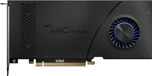
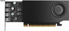
Intel Arc Pro A60
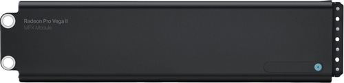
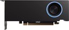
Radeon Pro Vega II
$2,800
|
2048 Shaders
12GB GDDR6
2050MHz
|
4096 Shaders
32GB HBM2
1720MHz
|
|
Peak AI Performance
268.7 TOPS
INT4 Tensor
|
Peak AI Performance
28.18 TFLOPS
FP16
|
|
FP32
8.4 TFLOPS
|
FP32
14.09 TFLOPS
|
|
FP16
16.79 TFLOPS
|
FP16
28.18 TFLOPS
|
|
Form Factor
PCIe Card
2.0-Slots
|
Form Factor
MPX
4.0-Slots
|
|
TDP
130W
|
TDP
300W
|
|
-
-
-
-
-
|
-
-
-
-
-
|
|
GB6 Metal N/A
0%
|
|
|
GB6 Vulkan N/A
0%
|
|
GB5 OpenCL N/A
0%
|
GB5 OpenCL N/A
0%
|
|
GB5 CUDA N/A
0%
|
GB5 CUDA N/A
0%
|
|
GB5 Metal N/A
0%
|
GB5 Metal N/A
0%
|
|
GB5 Vulkan N/A
0%
|
GB5 Vulkan N/A
0%
|
|
OCT 2020.1 N/A
0%
|
OCT 2020.1 N/A
0%
|
|
OCT Metal N/A
0%
|
OCT Metal N/A
0%
|
|
Peak AI
Performance
268.7 TOPS
INT4 Tensor
|
Peak AI
Performance
28.18 TFLOPS
FP16
|
|
-
-
-
|
-
-
-
|
|
-
-
-
-
-
-
|
-
-
-
-
-
-
|
|
FP16
16.79 TFLOPS
-
-
67.17 TFLOPS
Tensor (FP32 Accumulate)
-
|
FP16
28.18 TFLOPS
-
-
-
-
|
|
FP32
8.4 TFLOPS
-
-
|
FP32
14.09 TFLOPS
-
-
|
|
FP64
2.1 TFLOPS
-
|
FP64
3.52 TFLOPS
-
|
|
BF16
-
67.17 TFLOPS
Tensor
-
|
-
-
-
-
|
|
-
-
-
|
-
-
-
|
|
INT4
268.7 TOPS
Tensor
-
|
-
-
-
|
|
INT8
-
134.35 TOPS
Tensor
-
|
-
-
-
-
|
|
-
-
|
-
-
|
|
-
-
|
-
-
|
|
Pixel
Fillrate
131.2 GPixel/s
|
Pixel
Fillrate
110.08 GPixel/s
|
|
-
-
|
-
-
|
|
Texture
Fillrate
262.4 GTexel/s
|
Texture
Fillrate
440.32 GTexel/s
|
|
Manufacturer
Intel
|
Manufacturer
Apple
|
|
Chip Designer
Intel
|
Chip Designer
AMD
|
|
Architecture
Alchemist
|
Architecture
GCN 5
|
|
Family
Arc Pro A
|
Family
Radeon Pro Vega
|
|
Codename
Xe HPG
ACM-G12
Variant
DG2-256
|
Codename
Moonshot
Vega 20
Variant
Vega 20 XTXA
|
|
Market Segment
Workstation
|
Market Segment
Workstation
|
|
Release Date
6/6/2023
|
Release Date
12/1/2019
|
|
Foundry
TSMC
-
|
Foundry
TSMC
-
|
|
Fabrication Node
N6
-
|
Fabrication Node
N7
-
|
|
Die Size
269 mm²
-
|
Die Size
331 mm²
-
|
|
Transistor Count
11.5 Billion
-
|
Transistor Count
13.2 Billion
-
|
|
Transistor Density
42.75M/mm²
-
|
Transistor Density
39.97M/mm²
-
|
|
Form
PCIe Card
|
Form
MPX
|
|
Shading Units
2048 Shaders
-
|
Shading Units
4096 Shaders
-
|
|
Texture Mapping Units
128 TMUs
|
Texture Mapping Units
256 TMUs
|
|
Render Output Units
64 ROPs
|
Render Output Units
64 ROPs
|
|
Tensor Cores
256 T-Cores
|
-
-
|
|
Ray-Tracing Cores
16 RT-Cores
|
-
-
|
|
-
-
|
-
-
|
|
-
-
|
Compute Units
64 CUs
|
|
Execution Units
256 EUs
|
-
-
|
|
Graphics Processing Clusters
16 GPCs
|
-
-
|
|
-
-
900MHz Base
2050MHz
|
-
-
-
1720MHz
|
|
-
-
|
-
-
|
|
L1
-
-
-
Unknown
|
L1
-
-
16KB/CU
-
|
|
L2
8MB Shared
|
L2
4MB Shared
|
|
-
-
-
|
-
-
-
|
|
12GB
GDDR6
-
|
32GB
HBM2
-
|
|
Bus Width
192Bit
|
Bus Width
4096Bit
|
|
Clock
2000MHz
Transfer Rate
16GT/s
Bandwidth
384GB/s
|
Clock
1000MHz
Transfer Rate
2GT/s
Bandwidth
1024GB/s
|
|
-
-
-
-
-
-
-
-
-
|
-
-
-
-
-
-
-
-
-
|
|
TDP
130W
|
TDP
300W
|
|
-
-
|
-
-
|
|
-
-
-
-
-
-
-
-
-
-
-
-
-
-
-
-
-
-
4x mini-DisplayPort 2.0
-
-
-
-
-
-
-
-
-
-
-
-
-
-
-
-
-
-
-
-
|
-
-
-
-
-
-
-
-
-
-
-
-
-
-
-
-
-
-
-
-
-
-
-
-
-
-
-
-
-
-
-
-
-
-
-
1x HDMI 2.0
-
-
4x Thunderbolt 3 (40Gbps)
|
|
Max Resolution
7680x4320
|
Max Resolution
7680x4320
|
|
Max Resolution Refresh Rate
60Hz
|
Max Resolution Refresh Rate
60Hz
|
|
Variable Refresh Rate
-
FreeSync
-
|
Variable Refresh Rate
-
FreeSync
-
|
|
Display Stream Compression (DSC)
Not Supported
|
Display Stream Compression (DSC)
Not Supported
|
|
Multi Monitor Support
4
|
Multi Monitor Support
3
|
|
-
-
|
Content Protection
HDCP 2.2
|
|
Model
Arc
|
Model
VCE 4.1
|
|
Codec
-
-
-
-
-
-
-
-
AVC (H.264)
HEVC (H.265)
-
AV1
-
-
|
Codec
-
-
-
-
-
-
-
-
AVC (H.264)
HEVC (H.265)
-
-
-
-
|
|
Model
Arc
|
Model
UVD 7.2
|
|
Codec
-
MPEG-2
-
JPEG
-
-
VP9
-
AVC (H.264)
HEVC (H.265)
-
AV1
-
-
|
Codec
MPEG-1
MPEG-2
MPEG-4
JPEG
VC-1
-
-
-
AVC (H.264)
HEVC (H.265)
-
-
-
-
|
|
Direct X
12
Direct 3D
12_2
|
Direct X
12
Direct 3D
12_1
|
|
OpenGL
4.6
OpenCL
3.0
Vulkan
1.3
|
OpenGL
4.6
OpenCL
2.1
Vulkan
1.3
|
|
Shader Model
6.6
-
-
-
-
-
-
-
-
|
Shader Model
6.7
-
-
GFX
9
-
-
-
-
|
|
-
-
-
1x Fan
|
-
-
-
-
|
|
-
-
-
-
-
-
-
-
|
-
-
-
-
-
-
-
-
|
|
Slots Required
2.0
PCIe Version
4.0
PCIe Lanes
8
|
Slots Required
4.0
PCIe Version
3.0
PCIe Lanes
16
|
|
-
-
-
-
|
Multi GPU Support
Supported
Type
CrossFire XDMA
|
|
-
-
-
-
-
-
|
-
-
-
-
-
-
|


Copy Link