Intel Gaudi 3 vs AMD FirePro S7150
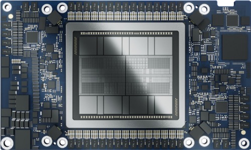
Intel Gaudi 3
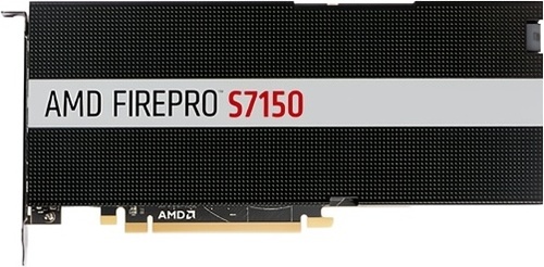
AMD FirePro S7150
$2,399
|
16384 Shaders
128GB HBM2e
438MHz
|
1792 Shaders
8GB GDDR5
1050MHz
|
|
Peak AI Performance
1.84 PFLOPS
FP8 Tensor (FP32 Accumulate)
|
Peak AI Performance
3.76 TFLOPS
FP32
|
|
FP32
14.35 TFLOPS
|
FP32
3.76 TFLOPS
|
|
FP16
28.7 TFLOPS
|
-
-
|
|
Form Factor
OAM Module
-
|
Form Factor
PCIe Card
1.0-Slots
|
|
TDP
900W
|
TDP
150W
|
|
-
-
-
-
-
|
Power Connectors
1x 6-Pin
-
-
-
|
|
GB6 OpenCL N/A
0%
|
|
|
GB6 Metal N/A
0%
|
GB6 Metal N/A
0%
|
|
GB6 Vulkan N/A
0%
|
|
GB5 OpenCL N/A
0%
|
GB5 OpenCL N/A
0%
|
|
GB5 CUDA N/A
0%
|
GB5 CUDA N/A
0%
|
|
GB5 Metal N/A
0%
|
GB5 Metal N/A
0%
|
|
GB5 Vulkan N/A
0%
|
GB5 Vulkan N/A
0%
|
|
OCT 2020.1 N/A
0%
|
OCT 2020.1 N/A
0%
|
|
OCT Metal N/A
0%
|
OCT Metal N/A
0%
|
|
Peak AI
Performance
1.84 PFLOPS
FP8 Tensor (FP32 Accumulate)
|
Peak AI
Performance
3.76 TFLOPS
FP32
|
|
-
-
-
|
-
-
-
|
|
FP8
-
-
-
1.84 PFLOPS
Tensor (FP32 Accumulate)
-
|
-
-
-
-
-
-
|
|
FP16
28.7 TFLOPS
-
-
458.75 TFLOPS
Tensor (FP32 Accumulate)
-
|
-
-
-
-
-
-
|
|
FP32
14.35 TFLOPS
229.38 TFLOPS
Tensor
-
|
FP32
3.76 TFLOPS
-
-
|
|
-
-
-
|
FP64
240 GFLOPS
-
|
|
BF16
28.7 TFLOPS
1.84 PFLOPS
Tensor
-
|
-
-
-
-
|
|
TF32
458.75 TFLOPS
Tensor
-
|
-
-
-
|
|
-
-
-
|
-
-
-
|
|
-
-
-
-
|
-
-
-
-
|
|
-
-
|
-
-
|
|
-
-
|
-
-
|
|
Pixel
Fillrate
-
|
Pixel
Fillrate
33.6 GPixel/s
|
|
-
-
|
-
-
|
|
Texture
Fillrate
-
|
Texture
Fillrate
117.6 GTexel/s
|
|
Foundry
TSMC
-
|
Foundry
TSMC
-
|
|
Fabrication Node
N5
-
|
Fabrication Node
28nm
-
|
|
-
-
-
|
Die Size
359 mm²
-
|
|
-
-
|
Transistor Count
5 Billion
-
|
|
-
-
-
|
Transistor Density
13.93M/mm²
-
|
|
Form
OAM Module
|
Form
PCIe Card
|
|
Shading Units
16384 Shaders
-
|
Shading Units
1792 Shaders
-
|
|
Texture Mapping Units
-
|
Texture Mapping Units
112 TMUs
|
|
Render Output Units
-
|
Render Output Units
32 ROPs
|
|
Tensor Cores
64 T-Cores
|
-
-
|
|
-
-
|
-
-
|
|
-
-
|
-
-
|
|
Compute Units
8 CUs
|
Compute Units
28 CUs
|
|
-
-
|
-
-
|
|
-
-
|
-
-
|
|
-
-
-
438MHz
|
-
-
-
1050MHz
|
|
-
-
|
-
-
|
|
L1
-
-
-
Unknown
|
L1
-
-
16KB/CU
-
|
|
L2
Unknown
|
L2
768KB Shared
|
|
-
-
-
|
-
-
-
|
|
128GB
HBM2e
ECC
|
8GB
GDDR5
-
|
|
Bus Width
8192Bit
|
Bus Width
256Bit
|
|
Clock
1808MHz
Transfer Rate
3.6GT/s
Bandwidth
3702.8GB/s
|
Clock
1250MHz
Transfer Rate
5GT/s
Bandwidth
160GB/s
|
|
-
-
-
-
eSRAM
96MB
12800GB/s
-
-
|
-
-
-
-
-
-
-
-
-
|
|
TDP
900W
|
TDP
150W
|
|
-
-
|
-
-
|
|
-
-
-
-
-
-
-
-
-
-
-
-
-
-
-
-
-
-
-
-
-
-
-
-
-
-
-
-
-
-
-
-
-
-
-
-
-
-
-
No Ports
|
-
-
-
-
-
-
-
-
-
-
-
-
-
-
-
-
-
-
-
-
-
-
-
-
-
-
-
-
-
-
-
-
-
-
-
-
-
-
-
No Ports
|
|
Max Resolution
Unknown
|
Max Resolution
4096x2160
|
|
Max Resolution Refresh Rate
-
|
Max Resolution Refresh Rate
60Hz
|
|
Variable Refresh Rate
-
-
-
|
Variable Refresh Rate
-
FreeSync
-
|
|
Display Stream Compression (DSC)
Not Supported
|
Display Stream Compression (DSC)
Not Supported
|
|
Multi Monitor Support
Unknown
|
Multi Monitor Support
3
|
|
-
-
|
Content Protection
HDCP 1.4
|
|
No Encoders
-
|
Model
VCE 3.0
|
|
-
-
-
-
-
-
-
-
-
-
-
-
-
-
-
|
Codec
-
-
-
-
-
-
-
-
AVC (H.264)
HEVC (H.265)
-
-
-
-
|
|
No Decoders
|
Model
UVD 5.0
|
|
-
-
-
-
-
-
-
-
-
-
-
-
-
-
|
Codec
MPEG-1
MPEG-2
MPEG-4
-
VC-1
-
-
-
AVC (H.264)
-
-
-
-
-
|
|
-
-
-
-
|
Direct X
12
Direct 3D
12_0
|
|
-
-
OpenCL
3.0
-
-
|
OpenGL
4.6
OpenCL
2.1
Vulkan
1.2
|
|
-
-
-
-
-
-
-
-
-
-
|
Shader Model
6.5
-
-
GFX
8
-
-
-
-
|
|
Not a Card
-
-
-
|
-
-
-
-
|
|
-
-
-
-
-
-
-
-
|
Power Connectors
-
-
1x 6-Pin
-
-
-
-
|
|
-
-
PCIe Version
5.0
PCIe Lanes
16
|
Slots Required
1.0
PCIe Version
3.0
PCIe Lanes
16
|
|
Multi GPU Support
Supported
Type
RoCE
|
Multi GPU Support
Supported
Type
CrossFire XDMA
|
|
-
-
-
-
-
-
|
Height
111 mm (4.37 in)
Width
241 mm (9.49 in)
Depth
20 mm (0.79 in)
|


Copy Link