NVIDIA A10 vs AMD FirePro S9300 X2

NVIDIA A10
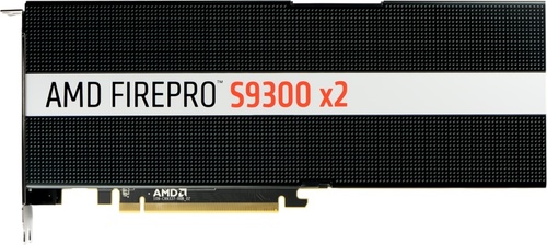
AMD FirePro S9300 X2
$5,999
|
9216 Shaders
24GB GDDR6
1695MHz
|
2x 4096 Shaders
8GB (2x 4GB) HBM
850MHz
|
|
Peak AI Performance
999.75 TOPS
INT4 Tensor Sparse
|
Peak AI Performance
13.93 TFLOPS
FP32
|
|
FP32
31.24 TFLOPS
|
FP32
13.93 TFLOPS
|
|
FP16
31.24 TFLOPS
|
-
-
|
|
Form Factor
PCIe Card
1.0-Slots
|
Form Factor
PCIe Card
2.0-Slots
|
|
TDP
150W
|
TDP
300W
|
|
Power Connectors
-
1x 8-Pin
-
-
|
Power Connectors
-
2x 8-Pin
-
-
|
|
GB6 OpenCL N/A
0%
|
|
|
GB6 Metal N/A
0%
|
GB6 Metal N/A
0%
|
|
GB6 Vulkan N/A
0%
|
GB6 Vulkan N/A
0%
|
|
GB5 OpenCL N/A
0%
|
GB5 OpenCL N/A
0%
|
|
GB5 CUDA N/A
0%
|
GB5 CUDA N/A
0%
|
|
GB5 Metal N/A
0%
|
GB5 Metal N/A
0%
|
|
GB5 Vulkan N/A
0%
|
GB5 Vulkan N/A
0%
|
|
OCT 2020.1 N/A
0%
|
OCT 2020.1 N/A
0%
|
|
OCT Metal N/A
0%
|
OCT Metal N/A
0%
|
|
Peak AI
Performance
999.75 TOPS
INT4 Tensor Sparse
|
Peak AI
Performance
13.93 TFLOPS
FP32
|
|
-
-
-
|
-
-
-
|
|
-
-
-
-
-
-
|
-
-
-
-
-
-
|
|
FP16
31.24 TFLOPS
124.97 TFLOPS
Tensor (FP16 Accumulate)
249.94 TFLOPS
Tensor (FP16 Accumulate) Sparse
124.97 TFLOPS
Tensor (FP32 Accumulate)
249.94 TFLOPS
Tensor (FP32 Accumulate) Sparse
|
-
-
-
-
-
-
|
|
FP32
31.24 TFLOPS
-
-
|
FP32
13.93 TFLOPS
-
-
|
|
FP64
490 GFLOPS
-
|
FP64
870 GFLOPS
-
|
|
BF16
31.24 TFLOPS
124.97 TFLOPS
Tensor
249.94 TFLOPS
Tensor Sparse
|
-
-
-
-
|
|
TF32
62.48 TFLOPS
Tensor
124.97 TFLOPS
Tensor Sparse
|
-
-
-
|
|
INT4
499.88 TOPS
Tensor
999.75 TOPS
Tensor Sparse
|
-
-
-
|
|
INT8
-
249.94 TOPS
Tensor
499.88 TOPS
Tensor Sparse
|
-
-
-
-
|
|
INT32
15.62 TOPS
|
-
-
|
|
Ray Tracing
61 TOPS
|
-
-
|
|
Pixel
Fillrate
162.72 GPixel/s
|
Pixel
Fillrate
54.4 GPixel/s
|
|
-
-
|
-
-
|
|
Texture
Fillrate
488.16 GTexel/s
|
Texture
Fillrate
217.6 GTexel/s
|
|
Manufacturer
NVIDIA
|
Manufacturer
AMD
|
|
Chip Designer
NVIDIA
|
Chip Designer
AMD
|
|
Architecture
Ampere
|
Architecture
GCN 3
|
|
Family
Server
|
Family
FirePro S
|
|
Codename
NV172
GA102
Variant
GA102-890-A1
|
Codename
Fiji
-
Variant
Capsaicin XT GL
|
|
Market Segment
Server
|
Market Segment
Server
|
|
Release Date
4/12/2021
|
Release Date
3/31/2016
|
|
Foundry
Samsung
-
|
Foundry
TSMC
-
|
|
Fabrication Node
8N
-
|
Fabrication Node
28nm
-
|
|
Die Size
628 mm²
-
|
Die Size
2x 596 mm²
-
|
|
Transistor Count
28.3 Billion
-
|
Transistor Count
2x 8.9 Billion
-
|
|
Transistor Density
45.04M/mm²
-
|
Transistor Density
14.93M/mm²
-
|
|
Form
PCIe Card
|
Form
PCIe Card
|
|
Shading Units
9216 Shaders
-
|
Shading Units
2x 4096 Shaders
-
|
|
Texture Mapping Units
288 TMUs
|
Texture Mapping Units
2x 256 TMUs
|
|
Render Output Units
96 ROPs
|
Render Output Units
2x 64 ROPs
|
|
Tensor Cores
288 T-Cores
|
-
-
|
|
Ray-Tracing Cores
72 RT-Cores
|
-
-
|
|
Streaming Multiprocessors
72 SMs
|
-
-
|
|
-
-
|
Compute Units
2x 64 CUs
|
|
-
-
|
-
-
|
|
-
-
|
-
-
|
|
-
-
885MHz Base
1695MHz
|
-
-
-
850MHz
|
|
-
-
|
-
-
|
|
L1
64KB/SM Tex
128KB/SM
-
-
|
L1
-
-
16KB/CU
-
|
|
L2
6MB Shared
|
L2
2MB Shared
|
|
-
-
-
|
-
-
-
|
|
24GB
GDDR6
-
|
8GB (2x 4GB)
HBM
-
|
|
Bus Width
384Bit
|
Bus Width
4096Bit
|
|
Clock
782MHz
Transfer Rate
6.3GT/s
Bandwidth
300.1GB/s
|
Clock
500MHz
Transfer Rate
1GT/s
Bandwidth
512GB/s
|
|
-
-
-
-
-
-
-
-
-
|
-
-
-
-
-
-
-
-
-
|
|
TDP
150W
|
TDP
300W
|
|
-
-
|
-
-
|
|
-
-
-
-
-
-
-
-
-
-
-
-
-
-
-
-
-
-
-
-
-
-
-
-
-
-
-
-
-
-
-
-
-
-
-
-
-
-
-
No Ports
|
-
-
-
-
-
-
-
-
-
-
-
-
-
-
-
-
-
-
-
-
-
-
-
-
-
-
-
-
-
-
-
-
-
-
-
-
-
-
-
No Ports
|
|
Max Resolution
Unknown
|
Max Resolution
4096x2160
|
|
Max Resolution Refresh Rate
-
|
Max Resolution Refresh Rate
60Hz
|
|
Variable Refresh Rate
G-Sync
FreeSync
-
|
Variable Refresh Rate
-
FreeSync
-
|
|
Display Stream Compression (DSC)
Not Supported
|
Display Stream Compression (DSC)
Not Supported
|
|
Multi Monitor Support
Unknown
|
Multi Monitor Support
4
|
|
-
-
|
Content Protection
HDCP 1.4
|
|
Model
NVENC 7
|
Model
VCE 3.0
|
|
Codec
-
-
-
-
-
-
-
-
AVC (H.264)
HEVC (H.265)
-
-
-
-
|
Codec
-
-
-
-
-
-
-
-
AVC (H.264)
HEVC (H.265)
-
-
-
-
|
|
Model
NVDEC 5
|
Model
UVD 6.0
|
|
Codec
MPEG-1
MPEG-2
MPEG-4
-
VC-1
VP8
VP9
-
AVC (H.264)
HEVC (H.265)
-
AV1
-
-
|
Codec
MPEG-1
MPEG-2
MPEG-4
JPEG
VC-1
-
-
-
AVC (H.264)
HEVC (H.265)
-
-
-
-
|
|
Direct X
12
Direct 3D
12_2
|
Direct X
12
Direct 3D
12_0
|
|
OpenGL
4.6
OpenCL
3.0
Vulkan
1.2
|
OpenGL
4.6
OpenCL
2.1
Vulkan
1.2
|
|
Shader Model
6.6
CUDA
8.6
-
-
PureVideo HD
VP11
VDPAU
Feature Set K
|
Shader Model
6.5
-
-
GFX
8
-
-
-
-
|
|
-
-
-
-
|
-
-
-
-
|
|
Power Connectors
-
-
-
1x 8-Pin
-
-
-
|
Power Connectors
-
-
-
2x 8-Pin
-
-
-
|
|
Slots Required
1.0
PCIe Version
4.0
PCIe Lanes
16
|
Slots Required
2.0
PCIe Version
3.0
PCIe Lanes
16
|
|
Multi GPU Support
Supported
Type
NVLink
|
Multi GPU Support
Supported
Type
CrossFire XDMA
|
|
Height
112 mm (4.41 in)
Width
267 mm (10.51 in)
Depth
20 mm (0.79 in)
|
Height
111 mm (4.37 in)
Width
267 mm (10.51 in)
Depth
37 mm (1.46 in)
|


Copy Link