NVIDIA A100X vs AMD FirePro S7100X
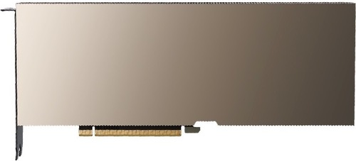
NVIDIA A100X
AMD FirePro S7100X
|
6912 Shaders
80GB HBM2e
1440MHz
|
2048 Shaders
8GB GDDR5
723MHz
|
|
Peak AI Performance
2.55 POPS
INT4 Tensor Sparse
|
Peak AI Performance
2.96 TFLOPS
FP32
|
|
FP32
19.91 TFLOPS
|
FP32
2.96 TFLOPS
|
|
FP16
79.63 TFLOPS
|
-
-
|
|
Form Factor
PCIe Card
2.0-Slots
|
Form Factor
MXM-A
-
|
|
TDP
300W
|
TDP
100W
|
|
Power Connectors
-
-
-
-
|
-
-
-
-
-
|
|
GB6 OpenCL N/A
0%
|
GB6 OpenCL N/A
0%
|
|
GB6 Metal N/A
0%
|
GB6 Metal N/A
0%
|
|
GB6 Vulkan N/A
0%
|
GB6 Vulkan N/A
0%
|
|
GB5 OpenCL N/A
0%
|
GB5 OpenCL N/A
0%
|
|
GB5 CUDA N/A
0%
|
GB5 CUDA N/A
0%
|
|
GB5 Metal N/A
0%
|
GB5 Metal N/A
0%
|
|
GB5 Vulkan N/A
0%
|
GB5 Vulkan N/A
0%
|
|
OCT 2020.1 N/A
0%
|
OCT 2020.1 N/A
0%
|
|
OCT Metal N/A
0%
|
OCT Metal N/A
0%
|
|
Peak AI
Performance
2.55 POPS
INT4 Tensor Sparse
|
Peak AI
Performance
2.96 TFLOPS
FP32
|
|
-
-
-
|
-
-
-
|
|
-
-
-
-
-
-
|
-
-
-
-
-
-
|
|
FP16
79.63 TFLOPS
318.51 TFLOPS
Tensor (FP16 Accumulate)
637.01 TFLOPS
Tensor (FP16 Accumulate) Sparse
318.51 TFLOPS
Tensor (FP32 Accumulate)
637.01 TFLOPS
Tensor (FP32 Accumulate) Sparse
|
-
-
-
-
-
-
|
|
FP32
19.91 TFLOPS
-
-
|
FP32
2.96 TFLOPS
-
-
|
|
FP64
9.95 TFLOPS
19.91 TFLOPS
Tensor
|
FP64
190 GFLOPS
-
|
|
BF16
39.81 TFLOPS
318.51 TFLOPS
Tensor
637.01 TFLOPS
Tensor Sparse
|
-
-
-
-
|
|
TF32
159.25 TFLOPS
Tensor
318.5 TFLOPS
Tensor Sparse
|
-
-
-
|
|
INT4
1.27 POPS
Tensor
2.55 POPS
Tensor Sparse
|
-
-
-
|
|
INT8
-
637.01 TOPS
Tensor
1.27 POPS
Tensor Sparse
|
-
-
-
-
|
|
INT32
19.91 TOPS
|
-
-
|
|
-
-
|
-
-
|
|
Pixel
Fillrate
230.4 GPixel/s
|
Pixel
Fillrate
23.136 GPixel/s
|
|
-
-
|
-
-
|
|
Texture
Fillrate
622.08 GTexel/s
|
Texture
Fillrate
92.544 GTexel/s
|
|
Manufacturer
NVIDIA
|
Manufacturer
AMD
|
|
Chip Designer
NVIDIA
|
Chip Designer
AMD
|
|
Architecture
Ampere
|
Architecture
GCN 3
|
|
Family
Server
|
Family
FirePro S
|
|
Codename
NV170
GA100
-
-
|
Codename
Tonga
-
Variant
Amethyst XT GL
|
|
Market Segment
Server
|
Market Segment
Server
|
|
Release Date
6/28/2021
|
Release Date
5/25/2016
|
|
Foundry
TSMC
-
|
Foundry
TSMC
-
|
|
Fabrication Node
7N
-
|
Fabrication Node
28nm
-
|
|
Die Size
826 mm²
-
|
Die Size
359 mm²
-
|
|
Transistor Count
54.2 Billion
-
|
Transistor Count
5 Billion
-
|
|
Transistor Density
65.62M/mm²
-
|
Transistor Density
13.93M/mm²
-
|
|
Form
PCIe Card
|
Form
MXM-A
|
|
Shading Units
6912 Shaders
-
|
Shading Units
2048 Shaders
-
|
|
Texture Mapping Units
432 TMUs
|
Texture Mapping Units
128 TMUs
|
|
Render Output Units
160 ROPs
|
Render Output Units
32 ROPs
|
|
Tensor Cores
432 T-Cores
|
-
-
|
|
-
-
|
-
-
|
|
Streaming Multiprocessors
108 SMs
|
-
-
|
|
-
-
|
Compute Units
32 CUs
|
|
-
-
|
-
-
|
|
-
-
|
-
-
|
|
-
-
795MHz Base
1440MHz
|
-
-
-
723MHz
|
|
-
-
|
-
-
|
|
L1
64KB/SM Tex
192KB/SM
-
-
|
L1
-
-
16KB/CU
-
|
|
L2
40MB Shared
|
L2
768KB Shared
|
|
-
-
-
|
-
-
-
|
|
80GB
HBM2e
-
|
8GB
GDDR5
-
|
|
Bus Width
5120Bit
|
Bus Width
256Bit
|
|
Clock
1593MHz
Transfer Rate
3.2GT/s
Bandwidth
2039GB/s
|
Clock
1050MHz
Transfer Rate
4.2GT/s
Bandwidth
134.4GB/s
|
|
-
-
-
-
-
-
-
-
-
|
-
-
-
-
-
-
-
-
-
|
|
TDP
300W
|
TDP
100W
|
|
-
-
|
-
-
|
|
-
-
-
-
-
-
-
-
-
-
-
-
-
-
-
-
-
-
-
-
-
-
-
-
-
-
-
-
-
-
-
-
-
-
-
-
-
-
-
No Ports
|
-
-
-
-
-
-
-
-
-
-
-
-
-
-
-
-
-
-
-
-
-
-
-
-
-
-
-
-
-
-
-
-
-
-
-
-
-
-
-
No Ports
|
|
Max Resolution
Unknown
|
Max Resolution
4096x2160
|
|
Max Resolution Refresh Rate
-
|
Max Resolution Refresh Rate
60Hz
|
|
Variable Refresh Rate
G-Sync
FreeSync
-
|
Variable Refresh Rate
-
FreeSync
-
|
|
Display Stream Compression (DSC)
Not Supported
|
Display Stream Compression (DSC)
Not Supported
|
|
Multi Monitor Support
Unknown
|
Multi Monitor Support
3
|
|
-
-
|
Content Protection
HDCP 1.4
|
|
No Encoders
-
|
Model
VCE 3.0
|
|
-
-
-
-
-
-
-
-
-
-
-
-
-
-
-
|
Codec
-
-
-
-
-
-
-
-
AVC (H.264)
HEVC (H.265)
-
-
-
-
|
|
Model
5x NVDEC 4
|
Model
UVD 5.0
|
|
Codec
MPEG-1
MPEG-2
MPEG-4
-
VC-1
VP8
VP9
-
AVC (H.264)
HEVC (H.265)
-
-
-
-
|
Codec
MPEG-1
MPEG-2
MPEG-4
-
VC-1
-
-
-
AVC (H.264)
-
-
-
-
-
|
|
-
-
-
-
|
Direct X
12
Direct 3D
12_0
|
|
-
-
OpenCL
3.0
Vulkan
1.2
|
OpenGL
4.6
OpenCL
2.1
Vulkan
1.2
|
|
-
-
CUDA
8.0
-
-
PureVideo HD
VP10
VDPAU
Feature Set J
|
Shader Model
6.5
-
-
GFX
8
-
-
-
-
|
|
-
-
-
-
|
Not a Card
-
-
-
|
|
Power Connectors
-
-
-
-
1x 8-Pin EPS
-
-
|
-
-
-
-
-
-
-
-
|
|
Slots Required
2.0
PCIe Version
4.0
PCIe Lanes
16
|
-
-
PCIe Version
3.0
PCIe Lanes
16
|
|
Multi GPU Support
Supported
Type
NVLink
|
-
-
-
-
|
|
Height
111 mm (4.37 in)
Width
267 mm (10.51 in)
Depth
40 mm (1.57 in)
|
-
-
-
-
-
-
|


Copy Link