NVIDIA A100X vs Intel Gaudi
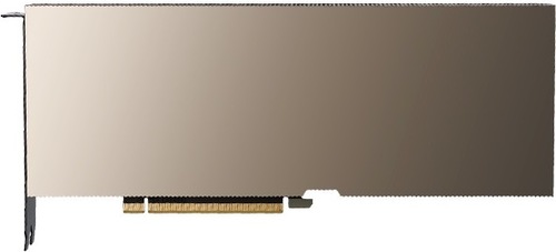
NVIDIA A100X
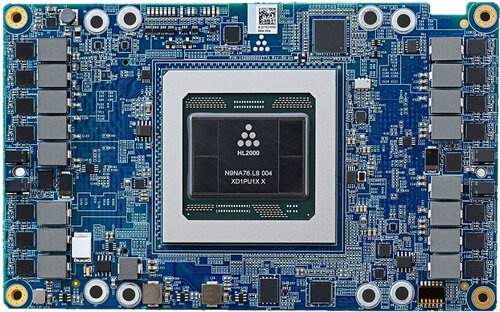
Intel Gaudi
|
6912 Shaders
80GB HBM2e
1440MHz
|
2048 Shaders
32GB HBM2
610MHz
|
|
Peak AI Performance
2.55 POPS
INT4 Tensor Sparse
|
Peak AI Performance
159.91 TFLOPS
BF16 Tensor
|
|
FP32
19.91 TFLOPS
|
-
-
|
|
FP16
79.63 TFLOPS
|
-
-
|
|
Form Factor
PCIe Card
2.0-Slots
|
Form Factor
OAM Module
-
|
|
TDP
300W
|
TDP
350W
|
|
Power Connectors
-
-
-
-
|
-
-
-
-
-
|
|
GB6 OpenCL N/A
0%
|
GB6 OpenCL N/A
0%
|
|
GB6 Metal N/A
0%
|
GB6 Metal N/A
0%
|
|
GB6 Vulkan N/A
0%
|
GB6 Vulkan N/A
0%
|
|
GB5 OpenCL N/A
0%
|
GB5 OpenCL N/A
0%
|
|
GB5 CUDA N/A
0%
|
GB5 CUDA N/A
0%
|
|
GB5 Metal N/A
0%
|
GB5 Metal N/A
0%
|
|
GB5 Vulkan N/A
0%
|
GB5 Vulkan N/A
0%
|
|
OCT 2020.1 N/A
0%
|
OCT 2020.1 N/A
0%
|
|
OCT Metal N/A
0%
|
OCT Metal N/A
0%
|
|
Peak AI
Performance
2.55 POPS
INT4 Tensor Sparse
|
Peak AI
Performance
159.91 TFLOPS
BF16 Tensor
|
|
-
-
-
|
-
-
-
|
|
-
-
-
-
-
-
|
-
-
-
-
-
-
|
|
FP16
79.63 TFLOPS
318.51 TFLOPS
Tensor (FP16 Accumulate)
637.01 TFLOPS
Tensor (FP16 Accumulate) Sparse
318.51 TFLOPS
Tensor (FP32 Accumulate)
637.01 TFLOPS
Tensor (FP32 Accumulate) Sparse
|
-
-
-
-
-
-
|
|
FP32
19.91 TFLOPS
-
-
|
-
-
-
-
|
|
FP64
9.95 TFLOPS
19.91 TFLOPS
Tensor
|
-
-
-
|
|
BF16
39.81 TFLOPS
318.51 TFLOPS
Tensor
637.01 TFLOPS
Tensor Sparse
|
BF16
-
159.91 TFLOPS
Tensor
-
|
|
TF32
159.25 TFLOPS
Tensor
318.5 TFLOPS
Tensor Sparse
|
-
-
-
|
|
INT4
1.27 POPS
Tensor
2.55 POPS
Tensor Sparse
|
-
-
-
|
|
INT8
-
637.01 TOPS
Tensor
1.27 POPS
Tensor Sparse
|
-
-
-
-
|
|
INT32
19.91 TOPS
|
-
-
|
|
-
-
|
-
-
|
|
Pixel
Fillrate
230.4 GPixel/s
|
Pixel
Fillrate
-
|
|
-
-
|
-
-
|
|
Texture
Fillrate
622.08 GTexel/s
|
Texture
Fillrate
-
|
|
Foundry
TSMC
-
|
Foundry
TSMC
-
|
|
Fabrication Node
7N
-
|
Fabrication Node
16FF
-
|
|
Die Size
826 mm²
-
|
-
-
-
|
|
Transistor Count
54.2 Billion
-
|
-
-
|
|
Transistor Density
65.62M/mm²
-
|
-
-
-
|
|
Form
PCIe Card
|
Form
OAM Module
|
|
Shading Units
6912 Shaders
-
|
Shading Units
2048 Shaders
-
|
|
Texture Mapping Units
432 TMUs
|
Texture Mapping Units
-
|
|
Render Output Units
160 ROPs
|
Render Output Units
-
|
|
Tensor Cores
432 T-Cores
|
Tensor Cores
8 T-Cores
|
|
-
-
|
-
-
|
|
Streaming Multiprocessors
108 SMs
|
-
-
|
|
-
-
|
Compute Units
1 CU
|
|
-
-
|
-
-
|
|
-
-
|
-
-
|
|
-
-
795MHz Base
1440MHz
|
-
-
-
610MHz
|
|
-
-
|
-
-
|
|
L1
64KB/SM Tex
192KB/SM
-
-
|
L1
-
-
-
Unknown
|
|
L2
40MB Shared
|
L2
Unknown
|
|
-
-
-
|
-
-
-
|
|
80GB
HBM2e
-
|
32GB
HBM2
ECC
|
|
Bus Width
5120Bit
|
Bus Width
4096Bit
|
|
Clock
1593MHz
Transfer Rate
3.2GT/s
Bandwidth
2039GB/s
|
Clock
980MHz
Transfer Rate
2GT/s
Bandwidth
1003.5GB/s
|
|
-
-
-
-
-
-
-
-
-
|
-
-
-
-
eSRAM
24MB
3200GB/s
-
-
|
|
TDP
300W
|
TDP
350W
|
|
-
-
|
-
-
|
|
-
-
-
-
-
-
-
-
-
-
-
-
-
-
-
-
-
-
-
-
-
-
-
-
-
-
-
-
-
-
-
-
-
-
-
-
-
-
-
No Ports
|
-
-
-
-
-
-
-
-
-
-
-
-
-
-
-
-
-
-
-
-
-
-
-
-
-
-
-
-
-
-
-
-
-
-
-
-
-
-
-
No Ports
|
|
Max Resolution
Unknown
|
Max Resolution
Unknown
|
|
Max Resolution Refresh Rate
-
|
Max Resolution Refresh Rate
-
|
|
Variable Refresh Rate
G-Sync
FreeSync
-
|
Variable Refresh Rate
-
-
-
|
|
Display Stream Compression (DSC)
Not Supported
|
Display Stream Compression (DSC)
Not Supported
|
|
Multi Monitor Support
Unknown
|
Multi Monitor Support
Unknown
|
|
-
-
|
-
-
|
|
No Encoders
-
|
No Encoders
-
|
|
-
-
-
-
-
-
-
-
-
-
-
-
-
-
-
|
-
-
-
-
-
-
-
-
-
-
-
-
-
-
-
|
|
Model
5x NVDEC 4
|
No Decoders
|
|
Codec
MPEG-1
MPEG-2
MPEG-4
-
VC-1
VP8
VP9
-
AVC (H.264)
HEVC (H.265)
-
-
-
-
|
-
-
-
-
-
-
-
-
-
-
-
-
-
-
|
|
-
-
-
-
|
-
-
-
-
|
|
-
-
OpenCL
3.0
Vulkan
1.2
|
-
-
OpenCL
3.0
-
-
|
|
-
-
CUDA
8.0
-
-
PureVideo HD
VP10
VDPAU
Feature Set J
|
-
-
-
-
-
-
-
-
-
-
|
|
-
-
-
-
|
Not a Card
-
-
-
|
|
Power Connectors
-
-
-
-
1x 8-Pin EPS
-
-
|
-
-
-
-
-
-
-
-
|
|
Slots Required
2.0
PCIe Version
4.0
PCIe Lanes
16
|
-
-
PCIe Version
4.0
PCIe Lanes
16
|
|
Multi GPU Support
Supported
Type
NVLink
|
Multi GPU Support
Supported
Type
RoCE
|
|
Height
111 mm (4.37 in)
Width
267 mm (10.51 in)
Depth
40 mm (1.57 in)
|
-
-
-
-
-
-
|


Copy Link