NVIDIA GB10 vs ATI 3D Rage II
NVIDIA GB10
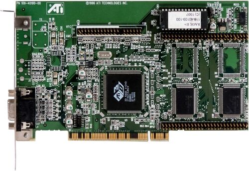
ATI 3D Rage II
|
6144 Shaders
Shared Memory
2525MHz
|
1 Shader
4MB SGRAM
60MHz
|
|
Peak AI Performance
992.87 TFLOPS
FP4 Tensor Sparse
|
Peak AI Performance
-
|
|
FP32
31.03 TFLOPS
|
-
-
|
|
FP16
62.05 TFLOPS
|
-
-
|
|
Form Factor
iGPU
-
|
Form Factor
PCI Card
1.0-Slots
|
|
TDP
Unknown
|
TDP
Unknown
|
|
-
-
-
-
-
|
-
-
-
-
-
|
|
GB6 OpenCL N/A
0%
|
GB6 OpenCL N/A
0%
|
|
GB6 Metal N/A
0%
|
GB6 Metal N/A
0%
|
|
GB6 Vulkan N/A
0%
|
GB6 Vulkan N/A
0%
|
|
GB5 OpenCL N/A
0%
|
GB5 OpenCL N/A
0%
|
|
GB5 CUDA N/A
0%
|
GB5 CUDA N/A
0%
|
|
GB5 Metal N/A
0%
|
GB5 Metal N/A
0%
|
|
GB5 Vulkan N/A
0%
|
GB5 Vulkan N/A
0%
|
|
OCT 2020.1 N/A
0%
|
OCT 2020.1 N/A
0%
|
|
OCT Metal N/A
0%
|
OCT Metal N/A
0%
|
|
Peak AI
Performance
992.87 TFLOPS
FP4 Tensor Sparse
|
Peak AI
Performance
-
|
|
FP4
496.44 TFLOPS
Tensor
992.87 TFLOPS
Tensor Sparse
|
-
-
-
|
|
FP8
-
248.22 TFLOPS
Tensor (FP16 Accumulate)
496.44 TFLOPS
Tensor (FP16 Accumulate) Sparse
124.11 TFLOPS
Tensor (FP32 Accumulate)
248.22 TFLOPS
Tensor (FP32 Accumulate) Sparse
|
-
-
-
-
-
-
|
|
FP16
62.05 TFLOPS
124.11 TFLOPS
Tensor (FP16 Accumulate)
248.22 TFLOPS
Tensor (FP16 Accumulate) Sparse
62.05 TFLOPS
Tensor (FP32 Accumulate)
124.11 TFLOPS
Tensor (FP32 Accumulate) Sparse
|
-
-
-
-
-
-
|
|
FP32
31.03 TFLOPS
-
-
|
-
-
-
-
|
|
FP64
15.51 TFLOPS
-
|
-
-
-
|
|
BF16
62.05 TFLOPS
62.05 TFLOPS
Tensor
124.11 TFLOPS
Tensor Sparse
|
-
-
-
-
|
|
TF32
31.03 TFLOPS
Tensor
62.05 TFLOPS
Tensor Sparse
|
-
-
-
|
|
-
-
-
|
-
-
-
|
|
INT8
-
248.22 TOPS
Tensor
496.44 TOPS
Tensor Sparse
|
-
-
-
-
|
|
INT32
31.03 TOPS
|
-
-
|
|
Ray Tracing
94.1 TOPS
|
-
-
|
|
Pixel
Fillrate
80.8 GPixel/s
|
Pixel
Fillrate
0.06 GPixel/s
|
|
-
-
|
-
-
|
|
Texture
Fillrate
484.8 GTexel/s
|
Texture
Fillrate
0.06 GTexel/s
|
|
-
-
-
|
Foundry
UMC
-
|
|
-
-
-
|
Fabrication Node
350nm
-
|
|
-
-
-
|
Die Size
39 mm²
-
|
|
-
-
|
Transistor Count
5 Million
-
|
|
-
-
-
|
Transistor Density
0.13M/mm²
-
|
|
Form
iGPU
|
Form
PCI Card
|
|
Shading Units
6144 Shaders
-
|
Shading Units
1 Shader
-
|
|
Texture Mapping Units
192 TMUs
|
Texture Mapping Units
1 TMU
|
|
Render Output Units
32 ROPs
|
Render Output Units
1 ROP
|
|
Tensor Cores
192 T-Cores
|
-
-
|
|
Ray-Tracing Cores
48 RT-Cores
|
-
-
|
|
Streaming Multiprocessors
48 SMs
|
-
-
|
|
-
-
|
-
-
|
|
-
-
|
-
-
|
|
-
-
|
-
-
|
|
-
-
2418MHz Base
2525MHz
|
-
-
-
60MHz
|
|
-
-
|
-
-
|
|
L1
64KB/SM Tex
256KB/SM
-
-
|
L1
-
-
-
Unknown
|
|
L2
24MB Shared
|
L2
Unknown
|
|
-
-
-
|
-
-
-
|
|
Shared Memory
-
-
|
4MB
SGRAM
-
|
|
-
|
Bus Width
64Bit
|
|
-
-
-
-
-
-
|
Clock
83MHz
Transfer Rate
83MT/s
Bandwidth
0.7GB/s
|
|
-
-
-
-
-
-
-
-
-
|
-
-
-
-
-
-
-
-
-
|
|
TDP
Unknown
|
TDP
Unknown
|
|
-
-
|
-
-
|
|
-
-
-
-
-
-
-
-
-
-
-
-
-
-
-
-
-
-
-
-
-
-
-
-
-
-
-
-
-
-
-
-
-
-
-
-
-
-
-
No Ports
|
1x VGA
-
-
-
-
-
-
-
-
-
-
-
-
-
-
-
-
-
-
-
-
-
-
-
-
-
-
-
-
-
-
-
-
-
-
-
-
-
-
|
|
Max Resolution
7680x4320
|
Max Resolution
640x480
|
|
Max Resolution Refresh Rate
165Hz
|
Max Resolution Refresh Rate
60Hz
|
|
Variable Refresh Rate
-
-
-
|
Variable Refresh Rate
-
-
-
|
|
Display Stream Compression (DSC)
Supported
|
Display Stream Compression (DSC)
Not Supported
|
|
Multi Monitor Support
4
|
Multi Monitor Support
1
|
|
Content Protection
HDCP 2.3
|
-
-
|
|
Model
NVENC 9
|
No Encoders
-
|
|
Codec
-
-
-
-
-
-
-
-
AVC (H.264)
HEVC (H.265)
-
AV1
-
-
|
-
-
-
-
-
-
-
-
-
-
-
-
-
-
-
|
|
Model
NVDEC 6
|
No Decoders
|
|
Codec
MPEG-1
MPEG-2
MPEG-4
-
VC-1
VP8
VP9
-
AVC (H.264)
HEVC (H.265)
-
AV1
-
-
|
-
-
-
-
-
-
-
-
-
-
-
-
-
-
|
|
Direct X
12
Direct 3D
12_3
|
Direct X
5
Direct 3D
5.0
|
|
OpenGL
4.6
OpenCL
3.0
Vulkan
1.3
|
-
-
-
-
-
-
|
|
Shader Model
6.8
CUDA
13.0
-
-
PureVideo HD
VP13
VDPAU
Feature Set M
|
-
-
-
-
-
-
-
-
-
-
|
|
Not a Card
-
-
-
|
-
-
-
-
|
|
-
-
-
-
-
-
-
-
|
-
-
-
-
-
-
-
-
|
|
-
-
-
-
-
-
|
Slots Required
1.0
-
-
-
-
|
|
-
-
-
-
|
-
-
-
-
|
|
-
-
-
-
-
-
|
-
-
-
-
-
-
|
Copy Link