NVIDIA GeForce GTX 1060 vs Radeon Pro 555
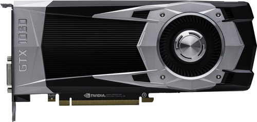
NVIDIA GeForce GTX 1060
$299

Radeon Pro 555
|
1280 Shaders
6GB GDDR5
1708MHz
|
768 Shaders
2GB GDDR5
850MHz
|
|
Peak AI Performance
17.49 TOPS
INT8
|
Peak AI Performance
1.31 TFLOPS
FP16
|
|
FP32
4.37 TFLOPS
|
FP32
1.31 TFLOPS
|
|
FP16
70 GFLOPS
|
FP16
1.31 TFLOPS
|
|
Form Factor
PCIe Card
2.0-Slots
|
Form Factor
Soldered
-
|
|
TDP
120W
|
TDP
35W
|
|
Power Connectors
1x 6-Pin
-
-
-
|
-
-
-
-
-
|
|
GB6 Metal N/A
0%
|
|
|
GB6 Vulkan N/A
0%
|
|
GB5 OpenCL N/A
0%
|
GB5 OpenCL N/A
0%
|
|
GB5 CUDA N/A
0%
|
GB5 CUDA N/A
0%
|
|
GB5 Metal N/A
0%
|
GB5 Metal N/A
0%
|
|
GB5 Vulkan N/A
0%
|
GB5 Vulkan N/A
0%
|
|
OCT 2020.1 N/A
0%
|
OCT 2020.1 N/A
0%
|
|
OCT Metal N/A
0%
|
OCT Metal N/A
0%
|
|
Peak AI
Performance
17.49 TOPS
INT8
|
Peak AI
Performance
1.31 TFLOPS
FP16
|
|
-
-
-
|
-
-
-
|
|
-
-
-
-
-
-
|
-
-
-
-
-
-
|
|
FP16
70 GFLOPS
-
-
-
-
|
FP16
1.31 TFLOPS
-
-
-
-
|
|
FP32
4.37 TFLOPS
-
-
|
FP32
1.31 TFLOPS
-
-
|
|
FP64
140 GFLOPS
-
|
FP64
80 GFLOPS
-
|
|
-
-
-
-
|
-
-
-
-
|
|
-
-
-
|
-
-
-
|
|
-
-
-
|
-
-
-
|
|
INT8
17.49 TOPS
-
-
|
-
-
-
-
|
|
-
-
|
-
-
|
|
-
-
|
-
-
|
|
Pixel
Fillrate
81.984 GPixel/s
|
Pixel
Fillrate
13.6 GPixel/s
|
|
-
-
|
-
-
|
|
Texture
Fillrate
136.64 GTexel/s
|
Texture
Fillrate
40.8 GTexel/s
|
|
Manufacturer
NVIDIA
|
Manufacturer
Apple
|
|
Chip Designer
NVIDIA
|
Chip Designer
AMD
|
|
Architecture
Pascal
|
Architecture
GCN 4
|
|
Family
GeForce 10
|
Family
Radeon Pro
|
|
Codename
NV136
GP106
Variant
GP106-400-A1
|
Codename
Baffin
Polaris 21
Variant
Polaris 21 XLA
|
|
Market Segment
Desktop
|
Market Segment
Laptop
|
|
Release Date
7/19/2016
|
Release Date
6/6/2017
|
|
Foundry
TSMC
-
|
Foundry
GlobalFoundries
-
|
|
Fabrication Node
16FF
-
|
Fabrication Node
14LPP
-
|
|
Die Size
200 mm²
-
|
Die Size
123 mm²
-
|
|
Transistor Count
4.4 Billion
-
|
Transistor Count
3 Billion
-
|
|
Transistor Density
22.00M/mm²
-
|
Transistor Density
24.39M/mm²
-
|
|
Form
PCIe Card
|
Form
Soldered
|
|
Shading Units
1280 Shaders
-
|
Shading Units
768 Shaders
-
|
|
Texture Mapping Units
80 TMUs
|
Texture Mapping Units
48 TMUs
|
|
Render Output Units
48 ROPs
|
Render Output Units
16 ROPs
|
|
-
-
|
-
-
|
|
-
-
|
-
-
|
|
Streaming Multiprocessors
10 SMs
|
-
-
|
|
-
-
|
Compute Units
12 CUs
|
|
-
-
|
-
-
|
|
Graphics Processing Clusters
2 GPCs
|
-
-
|
|
-
-
1506MHz Base
1708MHz
|
-
-
-
850MHz
|
|
-
-
|
-
-
|
|
L1
-
48KB/SM
-
-
|
L1
-
-
16KB/CU
-
|
|
L2
1.5MB Shared
|
L2
1MB Shared
|
|
-
-
-
|
-
-
-
|
|
6GB
GDDR5
-
|
2GB
GDDR5
-
|
|
Bus Width
192Bit
|
Bus Width
128Bit
|
|
Clock
2000MHz
Transfer Rate
8GT/s
Bandwidth
192GB/s
|
Clock
1275MHz
Transfer Rate
5.1GT/s
Bandwidth
81.6GB/s
|
|
-
-
-
-
-
-
-
-
-
|
-
-
-
-
-
-
-
-
-
|
|
TDP
120W
|
TDP
35W
|
|
-
-
|
-
-
|
|
-
-
-
-
-
-
-
-
-
-
1x DVI-D Dual-Link
-
-
-
-
-
-
-
-
-
-
-
-
-
3x DisplayPort 1.4
-
-
-
-
-
-
-
-
-
-
1x HDMI 2.0
-
-
-
|
-
-
-
-
-
-
-
-
-
-
-
-
-
-
-
-
-
-
-
-
-
-
-
-
-
-
-
-
-
-
-
-
-
-
-
-
-
-
-
No Ports
|
|
Max Resolution
7680x4320
|
Max Resolution
5120x2880
|
|
Max Resolution Refresh Rate
30Hz
|
Max Resolution Refresh Rate
60Hz
|
|
Variable Refresh Rate
G-Sync
FreeSync
-
|
Variable Refresh Rate
-
FreeSync
-
|
|
Display Stream Compression (DSC)
Not Supported
|
Display Stream Compression (DSC)
Not Supported
|
|
Multi Monitor Support
3
|
Multi Monitor Support
3
|
|
-
-
|
Content Protection
HDCP 2.2
|
|
Model
NVENC 4
|
Model
VCE 3.4
|
|
Codec
-
-
-
-
-
-
-
-
AVC (H.264)
HEVC (H.265)
-
-
-
-
|
Codec
-
-
-
-
-
-
-
-
AVC (H.264)
HEVC (H.265)
-
-
-
-
|
|
Model
NVDEC 3
|
Model
UVD 6.3
|
|
Codec
MPEG-1
MPEG-2
MPEG-4
-
VC-1
-
VP9
-
AVC (H.264)
HEVC (H.265)
-
-
-
-
|
Codec
MPEG-1
MPEG-2
MPEG-4
JPEG
VC-1
-
-
-
AVC (H.264)
HEVC (H.265)
-
-
-
-
|
|
Direct X
12
Direct 3D
12_1
|
Direct X
12
Direct 3D
12_0
|
|
OpenGL
4.6
OpenCL
3.0
Vulkan
1.3
|
OpenGL
4.6
OpenCL
2.1
Vulkan
1.3
|
|
Shader Model
6.7
CUDA
6.1
-
-
PureVideo HD
VP8
VDPAU
Feature Set H
|
Shader Model
6.7
-
-
GFX
8
-
-
-
-
|
|
-
-
-
1x Fan
|
Not a Card
-
-
-
|
|
Power Connectors
-
-
1x 6-Pin
-
-
-
-
|
-
-
-
-
-
-
-
-
|
|
Slots Required
2.0
PCIe Version
3.0
PCIe Lanes
16
|
-
-
PCIe Version
3.0
PCIe Lanes
8
|
|
-
-
-
-
|
-
-
-
-
|
|
Height
112 mm (4.41 in)
Width
250 mm (9.84 in)
Depth
40 mm (1.57 in)
|
-
-
-
-
-
-
|


Copy Link