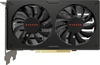
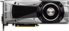
NVIDIA GeForce GTX 1650 GDDR5 vs AMD Radeon RX Vega 56

NVIDIA GeForce GTX 1650 GDDR5
$149
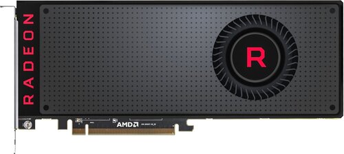
AMD Radeon RX Vega 56
$399
|
896 Shaders
4GB GDDR5
1665MHz
|
3584 Shaders
8GB HBM2
1471MHz
|
|
Peak AI Performance
5.97 TFLOPS
FP16
|
Peak AI Performance
21.09 TFLOPS
FP16
|
|
FP32
2.98 TFLOPS
|
FP32
10.54 TFLOPS
|
|
FP16
5.97 TFLOPS
|
FP16
21.09 TFLOPS
|
|
Form Factor
PCIe Card
-
|
Form Factor
PCIe Card
2.0-Slots
|
|
TDP
75W
|
TDP
210W
|
|
-
-
-
-
-
|
Power Connectors
-
2x 8-Pin
-
-
|
|
GB6 OpenCL N/A
0%
|
|
|
GB6 Metal N/A
0%
|
GB6 Metal 74,625
30%
|
|
GB6 Vulkan N/A
0%
|
GB6 Vulkan N/A
0%
|
|
GB5 OpenCL 37,005
12%
|
GB5 OpenCL N/A
0%
|
|
GB5 CUDA 38,480
11%
|
GB5 CUDA N/A
0%
|
|
GB5 Metal N/A
0%
|
GB5 Metal N/A
0%
|
|
GB5 Vulkan 33,805
16%
|
GB5 Vulkan N/A
0%
|
|
OCT 2020.1 75
10%
|
OCT 2020.1 N/A
0%
|
|
OCT Metal N/A
0%
|
OCT Metal N/A
0%
|
|
Peak AI
Performance
5.97 TFLOPS
FP16
|
Peak AI
Performance
21.09 TFLOPS
FP16
|
|
-
-
-
|
-
-
-
|
|
-
-
-
-
-
-
|
-
-
-
-
-
-
|
|
FP16
5.97 TFLOPS
-
-
-
-
|
FP16
21.09 TFLOPS
-
-
-
-
|
|
FP32
2.98 TFLOPS
-
-
|
FP32
10.54 TFLOPS
-
-
|
|
FP64
90 GFLOPS
-
|
FP64
660 GFLOPS
-
|
|
-
-
-
-
|
-
-
-
-
|
|
-
-
-
|
-
-
-
|
|
-
-
-
|
-
-
-
|
|
-
-
-
-
|
-
-
-
-
|
|
INT32
2.98 TOPS
|
-
-
|
|
-
-
|
-
-
|
|
Pixel
Fillrate
53.28 GPixel/s
|
Pixel
Fillrate
94.144 GPixel/s
|
|
-
-
|
-
-
|
|
Texture
Fillrate
93.24 GTexel/s
|
Texture
Fillrate
329.504 GTexel/s
|
|
Manufacturer
NVIDIA
|
Manufacturer
AMD
|
|
Chip Designer
NVIDIA
|
Chip Designer
AMD
|
|
Architecture
Turing
|
Architecture
GCN 5
|
|
Family
GeForce 16
|
Family
Radeon RX Vega
|
|
Codename
NV167
TU117
Variant
TU117-300-A1
|
Codename
Greenland
Vega 10
Variant
Vega 10 XL
|
|
Market Segment
Desktop
|
Market Segment
Desktop
|
|
Release Date
4/23/2019
|
Release Date
8/28/2017
|
|
Foundry
TSMC
-
|
Foundry
GlobalFoundries
-
|
|
Fabrication Node
12FFN
-
|
Fabrication Node
14LPP
-
|
|
Die Size
200 mm²
-
|
Die Size
486 mm²
-
|
|
Transistor Count
4.7 Billion
-
|
Transistor Count
12.5 Billion
-
|
|
Transistor Density
23.50M/mm²
-
|
Transistor Density
25.72M/mm²
-
|
|
Form
PCIe Card
|
Form
PCIe Card
|
|
Shading Units
896 Shaders
-
|
Shading Units
3584 Shaders
-
|
|
Texture Mapping Units
56 TMUs
|
Texture Mapping Units
224 TMUs
|
|
Render Output Units
32 ROPs
|
Render Output Units
64 ROPs
|
|
-
-
|
-
-
|
|
-
-
|
-
-
|
|
Streaming Multiprocessors
14 SMs
|
-
-
|
|
-
-
|
Compute Units
56 CUs
|
|
-
-
|
-
-
|
|
Graphics Processing Clusters
2 GPCs
|
-
-
|
|
-
-
1485MHz Base
1665MHz
|
-
-
1156MHz Base
1471MHz
|
|
-
-
|
-
-
|
|
L1
32KB/SM Tex
64KB/SM
-
-
|
L1
-
-
16KB/CU
-
|
|
L2
1MB Shared
|
L2
4MB Shared
|
|
-
-
-
|
-
-
-
|
|
4GB
GDDR5
-
|
8GB
HBM2
-
|
|
Bus Width
128Bit
|
Bus Width
2048Bit
|
|
Clock
2000MHz
Transfer Rate
8GT/s
Bandwidth
128GB/s
|
Clock
800MHz
Transfer Rate
1.6GT/s
Bandwidth
409.6GB/s
|
|
-
-
-
-
-
-
-
-
-
|
-
-
-
-
-
-
-
-
-
|
|
TDP
75W
|
TDP
210W
|
|
Temp
92°C Max
|
-
-
|
|
-
-
-
-
-
-
-
-
-
-
1x DVI-D Dual-Link
-
-
-
-
-
-
-
-
-
-
-
-
-
1x DisplayPort 1.4
-
-
-
-
-
-
-
-
-
-
1x HDMI 2.0
-
-
-
|
-
-
-
-
-
-
-
-
-
-
-
-
-
-
-
-
-
-
-
-
-
-
-
-
3x DisplayPort 1.4
-
-
-
-
-
-
-
-
-
-
1x HDMI 2.0
-
-
-
|
|
Max Resolution
7680x4320
|
Max Resolution
7680x4320
|
|
Max Resolution Refresh Rate
60Hz
|
Max Resolution Refresh Rate
60Hz
|
|
Variable Refresh Rate
G-Sync
FreeSync
-
|
Variable Refresh Rate
-
FreeSync
-
|
|
Display Stream Compression (DSC)
Supported
|
Display Stream Compression (DSC)
Not Supported
|
|
Multi Monitor Support
3
|
Multi Monitor Support
3
|
|
Content Protection
HDCP 2.2
|
Content Protection
HDCP 2.2
|
|
Model
NVENC 7
|
Model
VCE 4.0
|
|
Codec
-
-
-
-
-
-
-
-
AVC (H.264)
HEVC (H.265)
-
-
-
-
|
Codec
-
-
-
-
-
-
-
-
AVC (H.264)
HEVC (H.265)
-
-
-
-
|
|
Model
NVDEC 4
|
Model
UVD 7.0
|
|
Codec
MPEG-1
MPEG-2
MPEG-4
-
VC-1
VP8
VP9
-
AVC (H.264)
HEVC (H.265)
-
-
-
-
|
Codec
MPEG-1
MPEG-2
MPEG-4
JPEG
VC-1
-
-
-
AVC (H.264)
HEVC (H.265)
-
-
-
-
|
|
Direct X
12
Direct 3D
12_1
|
Direct X
12
Direct 3D
12_1
|
|
OpenGL
4.6
OpenCL
3.0
Vulkan
1.2
|
OpenGL
4.6
OpenCL
2.1
Vulkan
1.3
|
|
Shader Model
6.6
CUDA
7.5
-
-
PureVideo HD
VP10
VDPAU
Feature Set J
|
Shader Model
6.7
-
-
GFX
9
-
-
-
-
|
|
Not a Card
-
-
1x Fan
|
-
-
-
1x Fan
|
|
-
-
-
-
-
-
-
-
|
Power Connectors
-
-
-
2x 8-Pin
-
-
-
|
|
-
-
PCIe Version
3.0
PCIe Lanes
16
|
Slots Required
2.0
PCIe Version
3.0
PCIe Lanes
16
|
|
-
-
-
-
|
Multi GPU Support
Supported
Type
CrossFire XDMA
|
|
-
-
-
-
-
-
|
Height
111 mm (4.37 in)
Width
280 mm (11.02 in)
Depth
40 mm (1.57 in)
|


Copy Link