NVIDIA GeForce GTX 1660 vs NVIDIA GeForce GTX 950 OEM
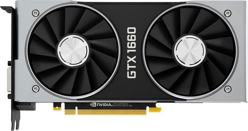
NVIDIA GeForce GTX 1660
$219

NVIDIA GeForce GTX 950 OEM
|
1408 Shaders
6GB GDDR5
1785MHz
|
1024 Shaders
2GB GDDR5
935MHz
|
|
Peak AI Performance
10.05 TFLOPS
FP16
|
Peak AI Performance
7.66 TOPS
INT8
|
|
FP32
5.03 TFLOPS
|
FP32
1.92 TFLOPS
|
|
FP16
10.05 TFLOPS
|
-
-
|
|
Form Factor
PCIe Card
-
|
Form Factor
PCIe Card
2.0-Slots
|
|
TDP
120W
|
TDP
Unknown
|
|
Power Connectors
-
1x 8-Pin
-
-
|
Power Connectors
1x 6-Pin
-
-
-
|
|
GB6 OpenCL N/A
0%
|
|
|
GB6 Metal N/A
0%
|
GB6 Metal N/A
0%
|
|
GB6 Vulkan N/A
0%
|
GB6 Vulkan N/A
0%
|
|
GB5 OpenCL 55,530
18%
|
GB5 OpenCL N/A
0%
|
|
GB5 CUDA 59,915
17%
|
GB5 CUDA N/A
0%
|
|
GB5 Metal N/A
0%
|
GB5 Metal N/A
0%
|
|
GB5 Vulkan 50,450
25%
|
GB5 Vulkan N/A
0%
|
|
OCT 2020.1 115
15%
|
OCT 2020.1 N/A
0%
|
|
OCT Metal N/A
0%
|
OCT Metal N/A
0%
|
|
Manufacturer
NVIDIA
|
Manufacturer
NVIDIA
|
|
Chip Designer
NVIDIA
|
Chip Designer
NVIDIA
|
|
Architecture
Turing
|
Architecture
Maxwell 2
|
|
Family
GeForce 16
|
Family
GeForce 900
|
|
Codename
NV168
TU116
Variant
TU116-300-A1
|
Codename
NV126
GM206
-
-
|
|
Market Segment
Desktop
|
Market Segment
Desktop
|
|
Release Date
3/14/2019
|
Release Date
8/20/2015
|
|
Foundry
TSMC
-
|
Foundry
TSMC
-
|
|
Fabrication Node
12FFN
-
|
Fabrication Node
28nm
-
|
|
Die Size
284 mm²
-
|
Die Size
227 mm²
-
|
|
Transistor Count
6.6 Billion
-
|
Transistor Count
8 Billion
-
|
|
Transistor Density
23.24M/mm²
-
|
Transistor Density
35.24M/mm²
-
|
|
Form
PCIe Card
|
Form
PCIe Card
|
|
Shading Units
1408 Shaders
-
|
Shading Units
1024 Shaders
-
|
|
Texture Mapping Units
88 TMUs
|
Texture Mapping Units
64 TMUs
|
|
Render Output Units
48 ROPs
|
Render Output Units
32 ROPs
|
|
-
-
|
-
-
|
|
-
-
|
-
-
|
|
Streaming Multiprocessors
22 SMs
|
Streaming Multiprocessors
8 SMs
|
|
-
-
|
-
-
|
|
-
-
|
-
-
|
|
Graphics Processing Clusters
3 GPCs
|
-
-
|
|
-
-
1530MHz Base
1785MHz
|
-
-
-
935MHz
|
|
Peak AI Performance
10.05 TFLOPS
FP16
|
Peak AI Performance
7.66 TOPS
INT8
|
|
-
-
-
|
-
-
-
|
|
-
-
-
-
-
-
|
-
-
-
-
-
-
|
|
FP16
10.05 TFLOPS
-
-
-
-
|
-
-
-
-
-
-
|
|
FP32
5.03 TFLOPS
-
-
|
FP32
1.92 TFLOPS
-
-
|
|
FP64
160 GFLOPS
-
|
FP64
60 GFLOPS
-
|
|
-
-
-
-
|
-
-
-
-
|
|
-
-
-
|
-
-
-
|
|
-
-
-
|
-
-
-
|
|
-
-
-
-
|
INT8
7.66 TOPS
-
-
|
|
INT32
5.03 TOPS
|
INT32
1.92 TOPS
|
|
-
-
|
-
-
|
|
Pixel Fillrate
85.68 GPixel/s
|
Pixel Fillrate
29.92 GPixel/s
|
|
-
-
|
-
-
|
|
Texture Fillrate
157.08 GTexel/s
|
Texture Fillrate
59.84 GTexel/s
|
|
-
-
|
-
-
|
|
L1
32KB/SM Tex
64KB/SM
-
-
|
L1
-
48KB/SM
-
-
|
|
L2
1.5MB Shared
|
L2
1MB Shared
|
|
-
-
-
|
-
-
-
|
|
6GB
GDDR5
-
|
2GB
GDDR5
-
|
|
Bus Width
192Bit
|
Bus Width
128Bit
|
|
Clock
2000MHz
Transfer Rate
8GT/s
Bandwidth
192GB/s
|
Clock
1250MHz
Transfer Rate
5GT/s
Bandwidth
80GB/s
|
|
-
-
-
-
-
-
-
-
-
|
-
-
-
-
-
-
-
-
-
|
|
TDP
120W
|
TDP
Unknown
|
|
Temp
95°C Max
|
-
-
|
|
-
-
-
-
-
-
-
-
-
-
1x DVI-D Dual-Link
-
-
-
-
-
-
-
-
-
-
-
-
-
1x DisplayPort 1.4
-
-
-
-
-
-
-
-
-
-
1x HDMI 2.0
-
-
-
|
-
-
-
-
-
-
-
-
1x DVI-I Dual-Link
-
-
-
-
-
-
-
-
-
-
-
-
-
3x DisplayPort 1.2
-
-
-
-
-
-
-
-
-
-
-
-
1x HDMI 2.0
-
-
-
|
|
Max Resolution
7680x4320
|
Max Resolution
4096x2304
|
|
Max Resolution Refresh Rate
60Hz
|
Max Resolution Refresh Rate
60Hz
|
|
Variable Refresh Rate
G-Sync
FreeSync
-
|
Variable Refresh Rate
G-Sync
FreeSync
-
|
|
Display Stream Compression (DSC)
Supported
|
Display Stream Compression (DSC)
Not Supported
|
|
Multi Monitor Support
3
|
Multi Monitor Support
3
|
|
Content Protection
HDCP 2.2
|
-
-
|
|
Model
NVENC 7
|
Model
NVENC 3
|
|
Codec
-
-
-
-
-
-
-
-
AVC (H.264)
HEVC (H.265)
-
-
-
-
|
Codec
-
-
-
-
-
-
-
-
AVC (H.264)
HEVC (H.265)
-
-
-
-
|
|
Model
NVDEC 4
|
Model
NVDEC 2
|
|
Codec
MPEG-1
MPEG-2
MPEG-4
-
VC-1
VP8
VP9
-
AVC (H.264)
HEVC (H.265)
-
-
-
-
|
Codec
MPEG-1
MPEG-2
MPEG-4
-
VC-1
VP8
VP9
-
AVC (H.264)
HEVC (H.265)
-
-
-
-
|
|
Direct X
12
Direct 3D
12_1
|
Direct X
12
Direct 3D
12_1
|
|
OpenGL
4.6
OpenCL
3.0
Vulkan
1.2
|
OpenGL
4.6
OpenCL
3.0
Vulkan
1.3
|
|
Shader Model
6.6
CUDA
7.5
-
-
PureVideo HD
VP10
VDPAU
Feature Set J
|
Shader Model
6.7
CUDA
5.2
-
-
PureVideo HD
VP7
VDPAU
Feature Set F
|
|
Not a Card
-
-
1x Fan
|
-
-
-
1x Fan
|
|
Power Connectors
-
-
-
1x 8-Pin
-
-
-
|
Power Connectors
-
-
1x 6-Pin
-
-
-
-
|
|
-
-
PCIe Version
3.0
PCIe Lanes
16
|
Slots Required
2.0
PCIe Version
3.0
PCIe Lanes
16
|
|
-
-
-
-
|
Multi GPU Support
Supported
Type
2-way SLI
|
|
-
-
-
-
-
-
|
Height
111 mm (4.37 in)
Width
202 mm (7.95 in)
Depth
38 mm (1.5 in)
|


Copy Link