NVIDIA GeForce RTX 2080 vs AMD Radeon 520
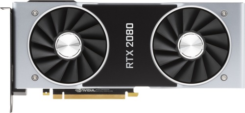
NVIDIA GeForce RTX 2080
$799

AMD Radeon 520
|
2944 Shaders
8GB GDDR6
1710MHz
|
320 Shaders
1GB GDDR5
1030MHz
|
|
Peak AI Performance
322.19 TOPS
INT4 Tensor
|
Peak AI Performance
660 GFLOPS
FP32
|
|
FP32
10.07 TFLOPS
|
FP32
660 GFLOPS
|
|
FP16
20.14 TFLOPS
|
-
-
|
|
Form Factor
PCIe Card
2.0-Slots
|
Form Factor
PCIe Card
1.0-Slots
|
|
TDP
215W
|
TDP
Unknown
|
|
Power Connectors
1x 6-Pin
1x 8-Pin
-
-
|
-
-
-
-
-
|
|
GB6 Metal N/A
0%
|
GB6 Metal N/A
0%
|
|
GB5 OpenCL 106,005
35%
|
GB5 OpenCL N/A
0%
|
|
GB5 CUDA 119,600
34%
|
GB5 CUDA N/A
0%
|
|
GB5 Metal N/A
0%
|
GB5 Metal N/A
0%
|
|
GB5 Vulkan 87,445
43%
|
GB5 Vulkan N/A
0%
|
|
OCT 2020.1 255
34%
|
OCT 2020.1 N/A
0%
|
|
OCT Metal N/A
0%
|
OCT Metal N/A
0%
|
|
Peak AI
Performance
322.19 TOPS
INT4 Tensor
|
Peak AI
Performance
660 GFLOPS
FP32
|
|
-
-
-
|
-
-
-
|
|
-
-
-
-
-
-
|
-
-
-
-
-
-
|
|
FP16
20.14 TFLOPS
80.55 TFLOPS
Tensor (FP16 Accumulate)
-
40.27 TFLOPS
Tensor (FP32 Accumulate)
-
|
-
-
-
-
-
-
|
|
FP32
10.07 TFLOPS
-
-
|
FP32
660 GFLOPS
-
-
|
|
FP64
320 GFLOPS
-
|
FP64
40 GFLOPS
-
|
|
BF16
-
40.27 TFLOPS
Tensor
-
|
-
-
-
-
|
|
TF32
40.27 TFLOPS
Tensor
-
|
-
-
-
|
|
INT4
322.19 TOPS
Tensor
-
|
-
-
-
|
|
INT8
-
161.1 TOPS
Tensor
-
|
-
-
-
-
|
|
INT32
10.07 TOPS
|
-
-
|
|
Ray Tracing
30.4 TOPS
|
-
-
|
|
Pixel
Fillrate
109.44 GPixel/s
|
Pixel
Fillrate
4.12 GPixel/s
|
|
-
-
|
-
-
|
|
Texture
Fillrate
314.64 GTexel/s
|
Texture
Fillrate
20.6 GTexel/s
|
|
Manufacturer
NVIDIA
|
Manufacturer
AMD
|
|
Chip Designer
NVIDIA
|
Chip Designer
AMD
|
|
Architecture
Turing
|
Architecture
GCN 1
|
|
Family
GeForce 20
|
Family
Radeon RX 500
|
|
Codename
NV164
TU104
Variant
TU104-400A-A1
|
Codename
Hainan
-
Variant
Banks Pro
|
|
Market Segment
Desktop
|
Market Segment
Desktop
|
|
Release Date
9/20/2018
|
Release Date
4/18/2017
|
|
Foundry
TSMC
-
|
Foundry
TSMC
-
|
|
Fabrication Node
12FFN
-
|
Fabrication Node
28nm
-
|
|
Die Size
545 mm²
-
|
Die Size
56 mm²
-
|
|
Transistor Count
13.6 Billion
-
|
Transistor Count
690 Million
-
|
|
Transistor Density
24.95M/mm²
-
|
Transistor Density
12.32M/mm²
-
|
|
Form
PCIe Card
|
Form
PCIe Card
|
|
Shading Units
2944 Shaders
-
|
Shading Units
320 Shaders
-
|
|
Texture Mapping Units
184 TMUs
|
Texture Mapping Units
20 TMUs
|
|
Render Output Units
64 ROPs
|
Render Output Units
4 ROPs
|
|
Tensor Cores
368 T-Cores
|
-
-
|
|
Ray-Tracing Cores
46 RT-Cores
|
-
-
|
|
Streaming Multiprocessors
46 SMs
|
-
-
|
|
-
-
|
Compute Units
5 CUs
|
|
-
-
|
-
-
|
|
Graphics Processing Clusters
6 GPCs
|
-
-
|
|
-
-
1515MHz Base
1710MHz
|
-
-
-
1030MHz
|
|
-
-
|
-
-
|
|
L1
32KB/SM Tex
64KB/SM
-
-
|
L1
-
-
16KB/CU
-
|
|
L2
4MB Shared
|
L2
128KB Shared
|
|
-
-
-
|
-
-
-
|
|
8GB
GDDR6
-
|
1GB
GDDR5
-
|
|
Bus Width
256Bit
|
Bus Width
64Bit
|
|
Clock
1750MHz
Transfer Rate
14GT/s
Bandwidth
448GB/s
|
Clock
1125MHz
Transfer Rate
4.5GT/s
Bandwidth
36GB/s
|
|
-
-
-
-
-
-
-
-
-
|
-
-
-
-
-
-
-
-
-
|
|
TDP
215W
|
TDP
Unknown
|
|
Temp
88°C Max
|
-
-
|
|
-
-
-
-
-
-
-
-
-
-
-
-
-
-
-
-
-
-
-
-
-
-
-
-
3x DisplayPort 1.4
-
-
-
-
-
-
-
-
-
-
1x HDMI 2.0
-
1x USB-C + DP
-
|
-
-
-
-
-
-
-
-
1x DVI-I Dual-Link
-
-
-
-
-
-
-
-
-
-
-
-
-
1x DisplayPort 1.2
-
-
-
-
-
-
-
-
-
-
-
-
-
-
-
-
|
|
Max Resolution
7680x4320
|
Max Resolution
4096x2160
|
|
Max Resolution Refresh Rate
60Hz
|
Max Resolution Refresh Rate
60Hz
|
|
Variable Refresh Rate
G-Sync
FreeSync
-
|
Variable Refresh Rate
-
-
-
|
|
Display Stream Compression (DSC)
Supported
|
Display Stream Compression (DSC)
Not Supported
|
|
Multi Monitor Support
4
|
Multi Monitor Support
3
|
|
Content Protection
HDCP 2.2
|
Content Protection
HDCP 1.4
|
|
Model
NVENC 7
|
No Encoders
-
|
|
Codec
-
-
-
-
-
-
-
-
AVC (H.264)
HEVC (H.265)
-
-
-
-
|
-
-
-
-
-
-
-
-
-
-
-
-
-
-
-
|
|
Model
NVDEC 4
|
No Decoders
|
|
Codec
MPEG-1
MPEG-2
MPEG-4
-
VC-1
VP8
VP9
-
AVC (H.264)
HEVC (H.265)
-
-
-
-
|
-
-
-
-
-
-
-
-
-
-
-
-
-
-
|
|
Direct X
12
Direct 3D
12_2
|
Direct X
12
Direct 3D
11_1
|
|
OpenGL
4.6
OpenCL
3.0
Vulkan
1.2
|
OpenGL
4.6
OpenCL
2.1
Vulkan
1.2
|
|
Shader Model
6.6
CUDA
7.5
-
-
PureVideo HD
VP10
VDPAU
Feature Set J
|
Shader Model
6.5
-
-
GFX
6
-
-
-
-
|
|
-
-
-
2x Fans
|
-
-
-
1x Fan
|
|
Power Connectors
-
-
1x 6-Pin
1x 8-Pin
-
-
-
|
-
-
-
-
-
-
-
-
|
|
Slots Required
2.0
PCIe Version
3.0
PCIe Lanes
16
|
Slots Required
1.0
PCIe Version
3.0
PCIe Lanes
8
|
|
Multi GPU Support
Supported
Type
2-way NVLink
|
-
-
-
-
|
|
Height
115.7 mm (4.56 in)
Width
266.7 mm (10.5 in)
Depth
35 mm (1.38 in)
|
-
-
-
-
-
-
|


Copy Link