NVIDIA GeForce RTX 3050 vs ATI Rage 128 PCI
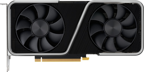
NVIDIA GeForce RTX 3050
$249
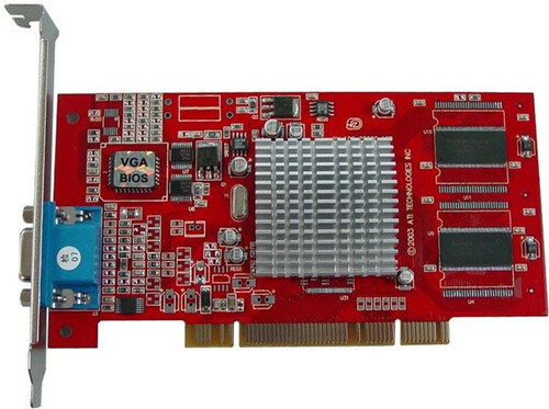
ATI Rage 128 PCI
|
2560 Shaders
8GB GDDR6
1777MHz
|
2 Shaders
16MB SGRAM
103MHz
|
|
Peak AI Performance
291.14 TOPS
INT4 Tensor Sparse
|
Peak AI Performance
-
|
|
FP32
9.1 TFLOPS
|
-
-
|
|
FP16
9.1 TFLOPS
|
-
-
|
|
Form Factor
PCIe Card
1.9-Slots
|
Form Factor
PCI Card
1.0-Slots
|
|
TDP
115W
|
TDP
Unknown
|
|
Power Connectors
-
-
1x 12-Pin
-
|
-
-
-
-
-
|
|
GB6 OpenCL N/A
0%
|
GB6 OpenCL N/A
0%
|
|
GB6 Metal N/A
0%
|
GB6 Metal N/A
0%
|
|
GB6 Vulkan N/A
0%
|
|
GB5 OpenCL 71,805
24%
|
GB5 OpenCL N/A
0%
|
|
GB5 CUDA 73,995
21%
|
GB5 CUDA N/A
0%
|
|
GB5 Metal N/A
0%
|
GB5 Metal N/A
0%
|
|
GB5 Vulkan 57,700
28%
|
GB5 Vulkan N/A
0%
|
|
OCT 2020.1 N/A
0%
|
OCT 2020.1 N/A
0%
|
|
OCT Metal N/A
0%
|
OCT Metal N/A
0%
|
|
Peak AI
Performance
291.14 TOPS
INT4 Tensor Sparse
|
Peak AI
Performance
-
|
|
-
-
-
|
-
-
-
|
|
-
-
-
-
-
-
|
-
-
-
-
-
-
|
|
FP16
9.1 TFLOPS
36.39 TFLOPS
Tensor (FP16 Accumulate)
72.79 TFLOPS
Tensor (FP16 Accumulate) Sparse
18.2 TFLOPS
Tensor (FP32 Accumulate)
36.39 TFLOPS
Tensor (FP32 Accumulate) Sparse
|
-
-
-
-
-
-
|
|
FP32
9.1 TFLOPS
-
-
|
-
-
-
-
|
|
FP64
140 GFLOPS
-
|
-
-
-
|
|
BF16
9.1 TFLOPS
18.2 TFLOPS
Tensor
36.39 TFLOPS
Tensor Sparse
|
-
-
-
-
|
|
TF32
9.1 TFLOPS
Tensor
18.2 TFLOPS
Tensor Sparse
|
-
-
-
|
|
INT4
145.57 TOPS
Tensor
291.14 TOPS
Tensor Sparse
|
-
-
-
|
|
INT8
-
72.79 TOPS
Tensor
145.57 TOPS
Tensor Sparse
|
-
-
-
-
|
|
INT32
4.55 TOPS
|
-
-
|
|
Ray Tracing
13.7 TOPS
|
-
-
|
|
Pixel
Fillrate
56.864 GPixel/s
|
Pixel
Fillrate
0.206 GPixel/s
|
|
-
-
|
-
-
|
|
Texture
Fillrate
142.16 GTexel/s
|
Texture
Fillrate
0.206 GTexel/s
|
|
Manufacturer
NVIDIA
|
Manufacturer
ATI
|
|
Chip Designer
NVIDIA
|
Chip Designer
ATI
|
|
Architecture
Ampere
|
Architecture
Rage 4
|
|
Family
GeForce 30
|
Family
Rage
|
|
Codename
NV177
GA107
Variant
GA107-150-A1
|
Codename
-
Rage 128
Variant
Rage 128
|
|
Market Segment
Desktop
|
Market Segment
Desktop
|
|
Release Date
12/16/2022
|
Release Date
8/1/1998
|
|
Foundry
Samsung
-
|
Foundry
TSMC
-
|
|
Fabrication Node
8N
-
|
Fabrication Node
250nm
-
|
|
Die Size
200 mm²
-
|
Die Size
89 mm²
-
|
|
Transistor Count
8.7 Billion
-
|
Transistor Count
17 Million
-
|
|
Transistor Density
43.50M/mm²
-
|
Transistor Density
0.19M/mm²
-
|
|
Form
PCIe Card
|
Form
PCI Card
|
|
Shading Units
2560 Shaders
-
|
Shading Units
2 Shaders
-
|
|
Texture Mapping Units
80 TMUs
|
Texture Mapping Units
2 TMUs
|
|
Render Output Units
32 ROPs
|
Render Output Units
2 ROPs
|
|
Tensor Cores
80 T-Cores
|
-
-
|
|
Ray-Tracing Cores
20 RT-Cores
|
-
-
|
|
Streaming Multiprocessors
20 SMs
|
-
-
|
|
-
-
|
-
-
|
|
-
-
|
-
-
|
|
Graphics Processing Clusters
2 GPCs
|
-
-
|
|
-
-
1552MHz Base
1777MHz
|
-
-
-
103MHz
|
|
-
-
|
-
-
|
|
L1
64KB/SM Tex
128KB/SM
-
-
|
L1
-
-
-
Unknown
|
|
L2
2MB Shared
|
L2
Unknown
|
|
-
-
-
|
-
-
-
|
|
8GB
GDDR6
-
|
16MB
SGRAM
-
|
|
Bus Width
128Bit
|
Bus Width
128Bit
|
|
Clock
1750MHz
Transfer Rate
14GT/s
Bandwidth
224GB/s
|
Clock
103MHz
Transfer Rate
103MT/s
Bandwidth
1.6GB/s
|
|
-
-
-
-
-
-
-
-
-
|
-
-
-
-
-
-
-
-
-
|
|
TDP
115W
|
TDP
Unknown
|
|
-
-
|
-
-
|
|
-
-
-
-
-
-
-
-
-
-
-
-
-
-
-
-
-
-
-
-
-
-
-
-
3x DisplayPort 1.4
-
-
-
-
-
-
-
-
-
-
-
1x HDMI 2.1
-
-
|
1x VGA
-
-
-
-
-
-
-
-
-
-
-
-
-
-
-
-
-
-
-
-
-
-
-
-
-
-
-
-
-
-
-
-
-
-
-
-
-
-
|
|
Max Resolution
7680x4320
|
Max Resolution
640x480
|
|
Max Resolution Refresh Rate
60Hz
|
Max Resolution Refresh Rate
60Hz
|
|
Variable Refresh Rate
G-Sync
FreeSync
-
|
Variable Refresh Rate
-
-
-
|
|
Display Stream Compression (DSC)
Supported
|
Display Stream Compression (DSC)
Not Supported
|
|
Multi Monitor Support
3
|
Multi Monitor Support
1
|
|
Content Protection
HDCP 2.3
|
-
-
|
|
Model
NVENC 7
|
No Encoders
-
|
|
Codec
-
-
-
-
-
-
-
-
AVC (H.264)
HEVC (H.265)
-
-
-
-
|
-
-
-
-
-
-
-
-
-
-
-
-
-
-
-
|
|
Model
NVDEC 5
|
No Decoders
|
|
Codec
MPEG-1
MPEG-2
MPEG-4
-
VC-1
VP8
VP9
-
AVC (H.264)
HEVC (H.265)
-
AV1
-
-
|
-
-
-
-
-
-
-
-
-
-
-
-
-
-
|
|
Direct X
12
Direct 3D
12_2
|
Direct X
6
Direct 3D
6.0
|
|
OpenGL
4.6
OpenCL
3.0
Vulkan
1.2
|
OpenGL
1.2
-
-
-
-
|
|
Shader Model
6.6
CUDA
8.6
-
-
PureVideo HD
VP11
VDPAU
Feature Set K
|
-
-
-
-
-
-
-
-
-
-
|
|
-
-
-
2x Fans
|
-
-
-
-
|
|
Power Connectors
-
-
-
-
-
1x 12-Pin
-
|
-
-
-
-
-
-
-
-
|
|
Slots Required
1.9
PCIe Version
4.0
PCIe Lanes
8
|
Slots Required
1.0
-
-
-
-
|
|
-
-
-
-
|
-
-
-
-
|
|
Height
112 mm (4.41 in)
Width
242 mm (9.53 in)
Depth
38 mm (1.5 in)
|
-
-
-
-
-
-
|

Copy Link