NVIDIA GeForce RTX 4060 vs NVIDIA GeForce RTX 3060

NVIDIA GeForce RTX 4060
$299
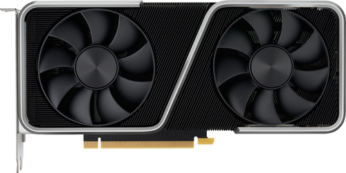
NVIDIA GeForce RTX 3060
$329
|
3072 Shaders
8GB GDDR6
2460MHz
|
3584 Shaders
12GB GDDR6
1777MHz
|
|
Peak AI Performance
483.66 TOPS
INT4 Tensor Sparse
|
Peak AI Performance
407.6 TOPS
INT4 Tensor Sparse
|
|
FP32
15.11 TFLOPS
|
FP32
12.74 TFLOPS
|
|
FP16
15.11 TFLOPS
|
FP16
12.74 TFLOPS
|
|
Form Factor
PCIe Card
2.1-Slots
|
Form Factor
PCIe Card
1.9-Slots
|
|
TDP
115W
|
TDP
170W
|
|
Power Connectors
-
-
-
1x 16-Pin 12VHPWR
|
Power Connectors
-
-
1x 12-Pin
-
|
|
GB6 Metal N/A
0%
|
GB6 Metal N/A
0%
|
|
GB5 OpenCL N/A
0%
|
GB5 OpenCL 96,465
32%
|
|
GB5 CUDA N/A
0%
|
GB5 CUDA 99,110
28%
|
|
GB5 Metal N/A
0%
|
GB5 Metal N/A
0%
|
|
GB5 Vulkan N/A
0%
|
GB5 Vulkan 75,845
37%
|
|
OCT 2020.1 N/A
0%
|
OCT 2020.1 305
40%
|
|
OCT Metal N/A
0%
|
OCT Metal N/A
0%
|
|
Peak AI
Performance
483.66 TOPS
INT4 Tensor Sparse
|
Peak AI
Performance
407.6 TOPS
INT4 Tensor Sparse
|
|
-
-
-
|
-
-
-
|
|
FP8
-
120.91 TFLOPS
Tensor (FP16 Accumulate)
241.83 TFLOPS
Tensor (FP16 Accumulate) Sparse
60.46 TFLOPS
Tensor (FP32 Accumulate)
120.91 TFLOPS
Tensor (FP32 Accumulate) Sparse
|
-
-
-
-
-
-
|
|
FP16
15.11 TFLOPS
60.46 TFLOPS
Tensor (FP16 Accumulate)
120.91 TFLOPS
Tensor (FP16 Accumulate) Sparse
30.23 TFLOPS
Tensor (FP32 Accumulate)
60.46 TFLOPS
Tensor (FP32 Accumulate) Sparse
|
FP16
12.74 TFLOPS
50.95 TFLOPS
Tensor (FP16 Accumulate)
101.9 TFLOPS
Tensor (FP16 Accumulate) Sparse
25.48 TFLOPS
Tensor (FP32 Accumulate)
50.95 TFLOPS
Tensor (FP32 Accumulate) Sparse
|
|
FP32
15.11 TFLOPS
-
-
|
FP32
12.74 TFLOPS
-
-
|
|
FP64
240 GFLOPS
-
|
FP64
200 GFLOPS
-
|
|
BF16
15.11 TFLOPS
30.23 TFLOPS
Tensor
60.46 TFLOPS
Tensor Sparse
|
BF16
12.74 TFLOPS
25.48 TFLOPS
Tensor
50.95 TFLOPS
Tensor Sparse
|
|
TF32
15.11 TFLOPS
Tensor
30.23 TFLOPS
Tensor Sparse
|
TF32
12.74 TFLOPS
Tensor
25.48 TFLOPS
Tensor Sparse
|
|
INT4
241.83 TOPS
Tensor
483.66 TOPS
Tensor Sparse
|
INT4
203.8 TOPS
Tensor
407.6 TOPS
Tensor Sparse
|
|
INT8
-
120.91 TOPS
Tensor
241.83 TOPS
Tensor Sparse
|
INT8
-
101.9 TOPS
Tensor
203.8 TOPS
Tensor Sparse
|
|
INT32
7.56 TOPS
|
INT32
6.37 TOPS
|
|
Ray Tracing
34.9 TOPS
|
Ray Tracing
19.2 TOPS
|
|
Pixel
Fillrate
118.08 GPixel/s
|
Pixel
Fillrate
85.296 GPixel/s
|
|
-
-
|
-
-
|
|
Texture
Fillrate
236.16 GTexel/s
|
Texture
Fillrate
199.024 GTexel/s
|
|
Manufacturer
NVIDIA
|
Manufacturer
NVIDIA
|
|
Chip Designer
NVIDIA
|
Chip Designer
NVIDIA
|
|
Architecture
Ada Lovelace
|
Architecture
Ampere
|
|
Family
GeForce 40
|
Family
GeForce 30
|
|
Codename
NV187
AD107
Variant
AD107-400-A1
|
Codename
NV176
GA106
Variant
GA106-300-A1
|
|
Market Segment
Desktop
|
Market Segment
Desktop
|
|
Release Date
5/18/2023
|
Release Date
2/25/2021
|
|
Foundry
TSMC
-
|
Foundry
Samsung
-
|
|
Fabrication Node
4N
-
|
Fabrication Node
8N
-
|
|
Die Size
159 mm²
-
|
Die Size
276 mm²
-
|
|
Transistor Count
18.9 Billion
-
|
Transistor Count
13.3 Billion
-
|
|
Transistor Density
118.87M/mm²
-
|
Transistor Density
48.01M/mm²
-
|
|
Form
PCIe Card
|
Form
PCIe Card
|
|
Shading Units
3072 Shaders
-
|
Shading Units
3584 Shaders
-
|
|
Texture Mapping Units
96 TMUs
|
Texture Mapping Units
112 TMUs
|
|
Render Output Units
48 ROPs
|
Render Output Units
48 ROPs
|
|
Tensor Cores
96 T-Cores
|
Tensor Cores
112 T-Cores
|
|
Ray-Tracing Cores
24 RT-Cores
|
Ray-Tracing Cores
28 RT-Cores
|
|
Streaming Multiprocessors
24 SMs
|
Streaming Multiprocessors
28 SMs
|
|
-
-
|
-
-
|
|
-
-
|
-
-
|
|
Graphics Processing Clusters
2 GPCs
|
Graphics Processing Clusters
3 GPCs
|
|
-
-
1830MHz Base
2460MHz
|
-
-
1320MHz Base
1777MHz
|
|
-
-
|
-
-
|
|
L1
64KB/SM Tex
128KB/SM
-
-
|
L1
64KB/SM Tex
128KB/SM
-
-
|
|
L2
48MB Shared
|
L2
3MB Shared
|
|
-
-
-
|
-
-
-
|
|
8GB
GDDR6
-
|
12GB
GDDR6
-
|
|
Bus Width
128Bit
|
Bus Width
192Bit
|
|
Clock
2250MHz
Transfer Rate
18GT/s
Bandwidth
288GB/s
|
Clock
1875MHz
Transfer Rate
15GT/s
Bandwidth
360GB/s
|
|
-
-
-
-
-
-
-
-
-
|
-
-
-
-
-
-
-
-
-
|
|
TDP
115W
|
TDP
170W
|
|
Temp
90°C Max
|
Temp
93°C Max
|
|
-
-
-
-
-
-
-
-
-
-
-
-
-
-
-
-
-
-
-
-
-
-
-
-
3x DisplayPort 1.4
-
-
-
-
-
-
-
-
-
-
-
1x HDMI 2.1
-
-
|
-
-
-
-
-
-
-
-
-
-
-
-
-
-
-
-
-
-
-
-
-
-
-
-
3x DisplayPort 1.4
-
-
-
-
-
-
-
-
-
-
-
1x HDMI 2.1
-
-
|
|
Max Resolution
7680x4320
|
Max Resolution
7680x4320
|
|
Max Resolution Refresh Rate
60Hz
|
Max Resolution Refresh Rate
60Hz
|
|
Variable Refresh Rate
G-Sync
FreeSync
-
|
Variable Refresh Rate
G-Sync
FreeSync
-
|
|
Display Stream Compression (DSC)
Supported
|
Display Stream Compression (DSC)
Supported
|
|
Multi Monitor Support
4
|
Multi Monitor Support
4
|
|
Content Protection
HDCP 2.3
|
Content Protection
HDCP 2.3
|
|
Model
NVENC 8
|
Model
NVENC 7
|
|
Codec
-
-
-
-
-
-
-
-
AVC (H.264)
HEVC (H.265)
-
AV1
-
-
|
Codec
-
-
-
-
-
-
-
-
AVC (H.264)
HEVC (H.265)
-
-
-
-
|
|
Model
NVDEC 5
|
Model
NVDEC 5
|
|
Codec
MPEG-1
MPEG-2
MPEG-4
-
VC-1
VP8
VP9
-
AVC (H.264)
HEVC (H.265)
-
AV1
-
-
|
Codec
MPEG-1
MPEG-2
MPEG-4
-
VC-1
VP8
VP9
-
AVC (H.264)
HEVC (H.265)
-
AV1
-
-
|
|
Direct X
12
Direct 3D
12_3
|
Direct X
12
Direct 3D
12_2
|
|
OpenGL
4.6
OpenCL
3.0
Vulkan
1.3
|
OpenGL
4.6
OpenCL
3.0
Vulkan
1.2
|
|
Shader Model
6.6
CUDA
8.9
-
-
PureVideo HD
VP12
VDPAU
Feature Set L
|
Shader Model
6.6
CUDA
8.6
-
-
PureVideo HD
VP11
VDPAU
Feature Set K
|
|
-
-
-
2x Fans
|
-
-
-
2x Fans
|
|
Power Connectors
-
-
-
-
-
-
1x 16-Pin 12VHPWR
|
Power Connectors
-
-
-
-
-
1x 12-Pin
-
|
|
Slots Required
2.1
PCIe Version
4.0
PCIe Lanes
16
|
Slots Required
1.9
PCIe Version
4.0
PCIe Lanes
16
|
|
-
-
-
-
|
-
-
-
-
|
|
Height
98 mm (3.86 in)
Width
244 mm (9.61 in)
Depth
42 mm (1.65 in)
|
Height
112 mm (4.41 in)
Width
242 mm (9.53 in)
Depth
38 mm (1.5 in)
|


Copy Link