NVIDIA GeForce RTX 5070 Ti vs NVIDIA 6x GeForce RTX 4090
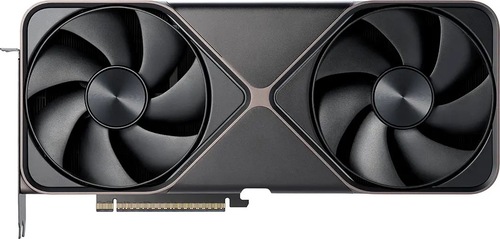
NVIDIA GeForce RTX 5070 Ti
$749
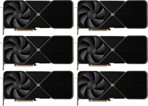
NVIDIA 6x GeForce RTX 4090
$9,594
|
8960 Shaders
16GB GDDR7
2452MHz
|
6x 16384 Shaders
144GB (6x 24GB) GDDR6X
2520MHz
|
|
Peak AI Performance
1.41 PFLOPS
FP4 Tensor Sparse
|
Peak AI Performance
15.85 POPS
INT4 Tensor Sparse
|
|
FP32
43.94 TFLOPS
|
FP32
495.45 TFLOPS
|
|
FP16
43.94 TFLOPS
|
FP16
495.45 TFLOPS
|
|
Form Factor
PCIe Card
2.1-Slots
|
Form Factor
PCIe Card
6x 3.0-Slots
|
|
TDP
300W
|
TDP
2700W
|
|
Power Connectors
-
-
-
1x 16-Pin 12VHPWR
|
Power Connectors
-
-
-
1x 16-Pin 12VHPWR
|
|
GB6 OpenCL N/A
0%
|
GB6 OpenCL N/A
0%
|
|
GB6 Metal N/A
0%
|
GB6 Metal N/A
0%
|
|
GB6 Vulkan N/A
0%
|
GB6 Vulkan N/A
0%
|
|
GB5 OpenCL N/A
0%
|
GB5 OpenCL N/A
0%
|
|
GB5 CUDA N/A
0%
|
GB5 CUDA N/A
0%
|
|
GB5 Metal N/A
0%
|
GB5 Metal N/A
0%
|
|
GB5 Vulkan N/A
0%
|
GB5 Vulkan N/A
0%
|
|
OCT 2020.1 N/A
0%
|
OCT 2020.1 N/A
0%
|
|
OCT Metal N/A
0%
|
OCT Metal N/A
0%
|
|
Peak AI
Performance
1.41 PFLOPS
FP4 Tensor Sparse
|
Peak AI
Performance
15.85 POPS
INT4 Tensor Sparse
|
|
FP4
703.04 TFLOPS
Tensor
1.41 PFLOPS
Tensor Sparse
|
-
-
-
|
|
FP8
-
351.52 TFLOPS
Tensor (FP16 Accumulate)
703.04 TFLOPS
Tensor (FP16 Accumulate) Sparse
175.76 TFLOPS
Tensor (FP32 Accumulate)
351.52 TFLOPS
Tensor (FP32 Accumulate) Sparse
|
FP8
-
3.96 PFLOPS
Tensor (FP16 Accumulate)
7.93 PFLOPS
Tensor (FP16 Accumulate) Sparse
1.98 PFLOPS
Tensor (FP32 Accumulate)
3.96 PFLOPS
Tensor (FP32 Accumulate) Sparse
|
|
FP16
43.94 TFLOPS
175.76 TFLOPS
Tensor (FP16 Accumulate)
351.52 TFLOPS
Tensor (FP16 Accumulate) Sparse
87.88 TFLOPS
Tensor (FP32 Accumulate)
175.76 TFLOPS
Tensor (FP32 Accumulate) Sparse
|
FP16
495.45 TFLOPS
1.98 PFLOPS
Tensor (FP16 Accumulate)
3.96 PFLOPS
Tensor (FP16 Accumulate) Sparse
990.91 TFLOPS
Tensor (FP32 Accumulate)
1.98 PFLOPS
Tensor (FP32 Accumulate) Sparse
|
|
FP32
43.94 TFLOPS
-
-
|
FP32
495.45 TFLOPS
-
-
|
|
FP64
690 GFLOPS
-
|
FP64
7.74 TFLOPS
-
|
|
BF16
43.94 TFLOPS
87.88 TFLOPS
Tensor
175.76 TFLOPS
Tensor Sparse
|
BF16
495.45 TFLOPS
990.91 TFLOPS
Tensor
1.98 PFLOPS
Tensor Sparse
|
|
TF32
43.94 TFLOPS
Tensor
87.88 TFLOPS
Tensor Sparse
|
TF32
495.45 TFLOPS
Tensor
990.9 TFLOPS
Tensor Sparse
|
|
-
-
-
|
INT4
7.93 POPS
Tensor
15.85 POPS
Tensor Sparse
|
|
INT8
-
351.52 TOPS
Tensor
703.04 TOPS
Tensor Sparse
|
INT8
-
3.96 POPS
Tensor
7.93 POPS
Tensor Sparse
|
|
INT32
43.94 TOPS
|
INT32
247.73 TOPS
|
|
Ray Tracing
133.3 TOPS
|
Ray Tracing
190.9 TOPS
|
|
Pixel
Fillrate
235.392 GPixel/s
|
Pixel
Fillrate
443.52 GPixel/s
|
|
-
-
|
-
-
|
|
Texture
Fillrate
686.56 GTexel/s
|
Texture
Fillrate
1290.24 GTexel/s
|
|
Manufacturer
NVIDIA
|
Manufacturer
NVIDIA
|
|
Chip Designer
NVIDIA
|
Chip Designer
NVIDIA
|
|
Architecture
Blackwell
|
Architecture
Ada Lovelace
|
|
Family
GeForce 50
|
Family
GeForce 40
|
|
Codename
NV193
GB203
Variant
GB203-200-A1
|
Codename
NV182
AD102
Variant
AD102-300-A1
|
|
Market Segment
Desktop
|
Market Segment
Desktop
|
|
Release Date
1/6/2025
|
Release Date
10/12/2022
|
|
Foundry
TSMC
-
|
Foundry
TSMC
-
|
|
Fabrication Node
4NP
-
|
Fabrication Node
4N
-
|
|
Die Size
378 mm²
-
|
Die Size
6x 608 mm²
-
|
|
Transistor Count
45.6 Billion
-
|
Transistor Count
6x 76.3 Billion
-
|
|
Transistor Density
120.63M/mm²
-
|
Transistor Density
125.41M/mm²
-
|
|
Form
PCIe Card
|
Form
PCIe Card
|
|
Shading Units
8960 Shaders
-
|
Shading Units
6x 16384 Shaders
-
|
|
Texture Mapping Units
280 TMUs
|
Texture Mapping Units
6x 512 TMUs
|
|
Render Output Units
96 ROPs
|
Render Output Units
6x 176 ROPs
|
|
Tensor Cores
280 T-Cores
|
Tensor Cores
6x 512 T-Cores
|
|
Ray-Tracing Cores
70 RT-Cores
|
Ray-Tracing Cores
6x 128 RT-Cores
|
|
Streaming Multiprocessors
70 SMs
|
Streaming Multiprocessors
6x 128 SMs
|
|
-
-
|
-
-
|
|
-
-
|
-
-
|
|
Graphics Processing Clusters
6 GPCs
|
Graphics Processing Clusters
6x 11 GPCs
|
|
-
-
2300MHz Base
2452MHz
|
-
-
2230MHz Base
2520MHz
|
|
-
-
|
-
-
|
|
L1
64KB/SM Tex
128KB/SM
-
-
|
L1
64KB/SM Tex
128KB/SM
-
-
|
|
L2
64MB Shared
|
L2
72MB Shared
|
|
-
-
-
|
-
-
-
|
|
16GB
GDDR7
-
|
144GB (6x 24GB)
GDDR6X
-
|
|
Bus Width
256Bit
|
Bus Width
384Bit
|
|
Clock
1750MHz
Transfer Rate
28GT/s
Bandwidth
896GB/s
|
Clock
1313MHz
Transfer Rate
21GT/s
Bandwidth
1008GB/s
|
|
-
-
-
-
-
-
-
-
-
|
-
-
-
-
-
-
-
-
-
|
|
TDP
300W
|
TDP
2700W
|
|
Temp
88°C Max
|
Temp
90°C Max
|
|
-
-
-
-
-
-
-
-
-
-
-
-
-
-
-
-
-
-
-
-
-
-
-
-
-
-
3x DisplayPort 2.1
-
-
-
-
-
-
-
-
-
1x HDMI 2.1
-
-
|
-
-
-
-
-
-
-
-
-
-
-
-
-
-
-
-
-
-
-
-
-
-
-
-
18x DisplayPort 1.4
-
-
-
-
-
-
-
-
-
-
-
6x HDMI 2.1
-
-
|
|
Max Resolution
7680x4320
|
Max Resolution
7680x4320
|
|
Max Resolution Refresh Rate
165Hz
|
Max Resolution Refresh Rate
60Hz
|
|
Variable Refresh Rate
G-Sync
FreeSync
-
|
Variable Refresh Rate
G-Sync
FreeSync
-
|
|
Display Stream Compression (DSC)
Supported
|
Display Stream Compression (DSC)
Supported
|
|
Multi Monitor Support
4
|
Multi Monitor Support
4
|
|
Content Protection
HDCP 2.3
|
Content Protection
HDCP 2.3
|
|
Model
2x NVENC 9
|
Model
2x NVENC 8
|
|
Codec
-
-
-
-
-
-
-
-
AVC (H.264)
HEVC (H.265)
-
AV1
-
-
|
Codec
-
-
-
-
-
-
-
-
AVC (H.264)
HEVC (H.265)
-
AV1
-
-
|
|
Model
NVDEC 6
|
Model
NVDEC 5
|
|
Codec
MPEG-1
MPEG-2
MPEG-4
-
VC-1
VP8
VP9
-
AVC (H.264)
HEVC (H.265)
-
AV1
-
-
|
Codec
MPEG-1
MPEG-2
MPEG-4
-
VC-1
VP8
VP9
-
AVC (H.264)
HEVC (H.265)
-
AV1
-
-
|
|
Direct X
12
Direct 3D
12_3
|
Direct X
12
Direct 3D
12_3
|
|
OpenGL
4.6
OpenCL
3.0
Vulkan
1.3
|
OpenGL
4.6
OpenCL
3.0
Vulkan
1.3
|
|
Shader Model
6.8
CUDA
12.8
-
-
PureVideo HD
VP13
VDPAU
Feature Set M
|
Shader Model
6.6
CUDA
8.9
-
-
PureVideo HD
VP12
VDPAU
Feature Set L
|
|
-
-
-
2x Fans
|
-
-
-
2x Fans
|
|
Power Connectors
-
-
-
-
-
-
1x 16-Pin 12VHPWR
|
Power Connectors
-
-
-
-
-
-
1x 16-Pin 12VHPWR
|
|
Slots Required
2.1
PCIe Version
5.0
PCIe Lanes
16
|
Slots Required
3.0
PCIe Version
4.0
PCIe Lanes
16
|
|
-
-
-
-
|
-
-
-
-
|
|
Height
137 mm (5.39 in)
Width
304 mm (11.97 in)
Depth
42 mm (1.65 in)
|
Height
137 mm (5.39 in)
Width
304 mm (11.97 in)
Depth
61 mm (2.4 in)
|


Copy Link