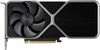
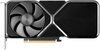
NVIDIA GeForce RTX 5070 vs ZOTAC GeForce RTX 3090 Trinity OC
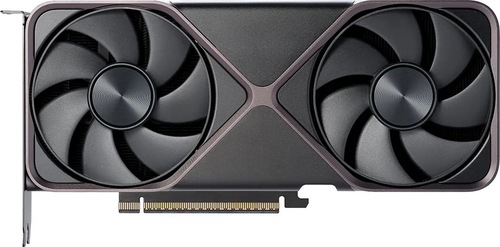
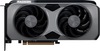
NVIDIA GeForce RTX 5070
$549
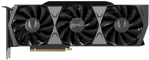
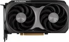
ZOTAC GeForce RTX 3090 Trinity OC
$950
|
6144 Shaders
12GB GDDR7
2512MHz
|
10496 Shaders
24GB GDDR6X
1710MHz
|
|
Peak AI Performance
987.76 TFLOPS
FP4 Tensor Sparse
|
Peak AI Performance
1.15 POPS
INT4 Tensor Sparse
|
|
FP32
30.87 TFLOPS
|
FP32
35.9 TFLOPS
|
|
FP16
30.87 TFLOPS
|
FP16
35.9 TFLOPS
|
|
Form Factor
PCIe Card
2.1-Slots
|
Form Factor
PCIe Card
2.9-Slots
|
|
TDP
250W
|
TDP
350W
|
|
Power Connectors
-
-
-
1x 16-Pin 12VHPWR
|
Power Connectors
-
2x 8-Pin
-
-
|
|
GB6 OpenCL N/A
0%
|
GB6 OpenCL N/A
0%
|
|
GB6 Metal N/A
0%
|
GB6 Metal N/A
0%
|
|
GB6 Vulkan N/A
0%
|
GB6 Vulkan N/A
0%
|
|
GB5 OpenCL N/A
0%
|
GB5 OpenCL 207,255
68%
|
|
GB5 CUDA N/A
0%
|
GB5 CUDA 240,795
68%
|
|
GB5 Metal N/A
0%
|
GB5 Metal N/A
0%
|
|
GB5 Vulkan N/A
0%
|
GB5 Vulkan 139,425
68%
|
|
OCT 2020.1 N/A
0%
|
OCT 2020.1 660
87%
|
|
OCT Metal N/A
0%
|
OCT Metal N/A
0%
|
|
Peak AI
Performance
987.76 TFLOPS
FP4 Tensor Sparse
|
Peak AI
Performance
1.15 POPS
INT4 Tensor Sparse
|
|
FP4
493.88 TFLOPS
Tensor
987.76 TFLOPS
Tensor Sparse
|
-
-
-
|
|
FP8
-
246.94 TFLOPS
Tensor (FP16 Accumulate)
493.88 TFLOPS
Tensor (FP16 Accumulate) Sparse
123.47 TFLOPS
Tensor (FP32 Accumulate)
246.94 TFLOPS
Tensor (FP32 Accumulate) Sparse
|
-
-
-
-
-
-
|
|
FP16
30.87 TFLOPS
123.47 TFLOPS
Tensor (FP16 Accumulate)
246.94 TFLOPS
Tensor (FP16 Accumulate) Sparse
61.74 TFLOPS
Tensor (FP32 Accumulate)
123.47 TFLOPS
Tensor (FP32 Accumulate) Sparse
|
FP16
35.9 TFLOPS
143.59 TFLOPS
Tensor (FP16 Accumulate)
287.17 TFLOPS
Tensor (FP16 Accumulate) Sparse
71.79 TFLOPS
Tensor (FP32 Accumulate)
143.59 TFLOPS
Tensor (FP32 Accumulate) Sparse
|
|
FP32
30.87 TFLOPS
-
-
|
FP32
35.9 TFLOPS
-
-
|
|
FP64
480 GFLOPS
-
|
FP64
560 GFLOPS
-
|
|
BF16
30.87 TFLOPS
61.74 TFLOPS
Tensor
123.47 TFLOPS
Tensor Sparse
|
BF16
35.9 TFLOPS
71.79 TFLOPS
Tensor
143.59 TFLOPS
Tensor Sparse
|
|
TF32
30.87 TFLOPS
Tensor
61.73 TFLOPS
Tensor Sparse
|
TF32
35.9 TFLOPS
Tensor
71.79 TFLOPS
Tensor Sparse
|
|
-
-
-
|
INT4
574.34 TOPS
Tensor
1.15 POPS
Tensor Sparse
|
|
INT8
-
246.94 TOPS
Tensor
493.88 TOPS
Tensor Sparse
|
INT8
-
287.17 TOPS
Tensor
574.34 TOPS
Tensor Sparse
|
|
INT32
30.87 TOPS
|
INT32
17.95 TOPS
|
|
Ray Tracing
93.6 TOPS
|
Ray Tracing
70.1 TOPS
|
|
Pixel
Fillrate
200.96 GPixel/s
|
Pixel
Fillrate
191.52 GPixel/s
|
|
-
-
|
-
-
|
|
Texture
Fillrate
482.304 GTexel/s
|
Texture
Fillrate
560.88 GTexel/s
|
|
Manufacturer
NVIDIA
|
Manufacturer
ZOTAC
|
|
Chip Designer
NVIDIA
|
Chip Designer
NVIDIA
|
|
Architecture
Blackwell
|
Architecture
Ampere
|
|
Family
GeForce 50
|
Family
GeForce 30
|
|
Codename
NV195
GB205
Variant
GB205-300-A1
|
Codename
NV172
GA102
Variant
GA102-300-A1
|
|
Market Segment
Desktop
|
Market Segment
Desktop
|
|
Release Date
1/6/2025
|
Release Date
9/24/2020
|
|
Foundry
TSMC
-
|
Foundry
Samsung
-
|
|
Fabrication Node
4NP
-
|
Fabrication Node
8N
-
|
|
Die Size
263 mm²
-
|
Die Size
628 mm²
-
|
|
Transistor Count
31.1 Billion
-
|
Transistor Count
28.3 Billion
-
|
|
Transistor Density
118.25M/mm²
-
|
Transistor Density
45.04M/mm²
-
|
|
Form
PCIe Card
|
Form
PCIe Card
|
|
Shading Units
6144 Shaders
-
|
Shading Units
10496 Shaders
-
|
|
Texture Mapping Units
192 TMUs
|
Texture Mapping Units
328 TMUs
|
|
Render Output Units
80 ROPs
|
Render Output Units
112 ROPs
|
|
Tensor Cores
192 T-Cores
|
Tensor Cores
328 T-Cores
|
|
Ray-Tracing Cores
48 RT-Cores
|
Ray-Tracing Cores
82 RT-Cores
|
|
Streaming Multiprocessors
48 SMs
|
Streaming Multiprocessors
82 SMs
|
|
-
-
|
-
-
|
|
-
-
|
-
-
|
|
Graphics Processing Clusters
4 GPCs
|
Graphics Processing Clusters
7 GPCs
|
|
-
-
2160MHz Base
2512MHz
|
-
-
1395MHz Base
1710MHz
|
|
-
-
|
-
-
|
|
L1
64KB/SM Tex
128KB/SM
-
-
|
L1
64KB/SM Tex
128KB/SM
-
-
|
|
L2
40MB Shared
|
L2
6MB Shared
|
|
-
-
-
|
-
-
-
|
|
12GB
GDDR7
-
|
24GB
GDDR6X
-
|
|
Bus Width
192Bit
|
Bus Width
384Bit
|
|
Clock
1750MHz
Transfer Rate
28GT/s
Bandwidth
672GB/s
|
Clock
1219MHz
Transfer Rate
19.5GT/s
Bandwidth
936GB/s
|
|
-
-
-
-
-
-
-
-
-
|
-
-
-
-
-
-
-
-
-
|
|
TDP
250W
|
TDP
350W
|
|
Temp
85°C Max
|
Temp
93°C Max
|
|
-
-
-
-
-
-
-
-
-
-
-
-
-
-
-
-
-
-
-
-
-
-
-
-
-
-
3x DisplayPort 2.1
-
-
-
-
-
-
-
-
-
1x HDMI 2.1
-
-
|
-
-
-
-
-
-
-
-
-
-
-
-
-
-
-
-
-
-
-
-
-
-
-
-
3x DisplayPort 1.4
-
-
-
-
-
-
-
-
-
-
-
1x HDMI 2.1
-
-
|
|
Max Resolution
7680x4320
|
Max Resolution
7680x4320
|
|
Max Resolution Refresh Rate
165Hz
|
Max Resolution Refresh Rate
60Hz
|
|
Variable Refresh Rate
G-Sync
FreeSync
-
|
Variable Refresh Rate
G-Sync
FreeSync
-
|
|
Display Stream Compression (DSC)
Supported
|
Display Stream Compression (DSC)
Supported
|
|
Multi Monitor Support
4
|
Multi Monitor Support
4
|
|
Content Protection
HDCP 2.3
|
Content Protection
HDCP 2.3
|
|
Model
NVENC 9
|
Model
NVENC 7
|
|
Codec
-
-
-
-
-
-
-
-
AVC (H.264)
HEVC (H.265)
-
AV1
-
-
|
Codec
-
-
-
-
-
-
-
-
AVC (H.264)
HEVC (H.265)
-
-
-
-
|
|
Model
NVDEC 6
|
Model
NVDEC 5
|
|
Codec
MPEG-1
MPEG-2
MPEG-4
-
VC-1
VP8
VP9
-
AVC (H.264)
HEVC (H.265)
-
AV1
-
-
|
Codec
MPEG-1
MPEG-2
MPEG-4
-
VC-1
VP8
VP9
-
AVC (H.264)
HEVC (H.265)
-
AV1
-
-
|
|
Direct X
12
Direct 3D
12_3
|
Direct X
12
Direct 3D
12_2
|
|
OpenGL
4.6
OpenCL
3.0
Vulkan
1.3
|
OpenGL
4.6
OpenCL
3.0
Vulkan
1.2
|
|
Shader Model
6.8
CUDA
12.8
-
-
PureVideo HD
VP13
VDPAU
Feature Set M
|
Shader Model
6.6
CUDA
8.6
-
-
PureVideo HD
VP11
VDPAU
Feature Set K
|
|
-
-
-
2x Fans
|
-
-
-
3x Fans
|
|
Power Connectors
-
-
-
-
-
-
1x 16-Pin 12VHPWR
|
Power Connectors
-
-
-
2x 8-Pin
-
-
-
|
|
Slots Required
2.1
PCIe Version
5.0
PCIe Lanes
16
|
Slots Required
2.9
PCIe Version
4.0
PCIe Lanes
16
|
|
-
-
-
-
|
Multi GPU Support
Supported
Type
2-way NVLink
|
|
Height
112 mm (4.41 in)
Width
242 mm (9.53 in)
Depth
42 mm (1.65 in)
|
Height
120.7 mm (4.75 in)
Width
317.8 mm (12.51 in)
Depth
58 mm (2.28 in)
|


Copy Link