NVIDIA GeForce RTX 5080 vs XFX Radeon RX 6700 XT Speedster MERC 319
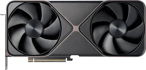
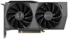
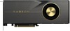
NVIDIA GeForce RTX 5080
$999

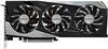
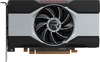
XFX Radeon RX 6700 XT Speedster MERC 319
$479
|
10752 Shaders
16GB GDDR7
2617MHz
|
2560 Shaders
12GB GDDR6
2622MHz
|
|
Peak AI Performance
1.8 PFLOPS
FP4 Tensor Sparse
|
Peak AI Performance
26.85 TFLOPS
FP16
|
|
FP32
56.28 TFLOPS
|
FP32
13.43 TFLOPS
|
|
FP16
56.28 TFLOPS
|
FP16
26.85 TFLOPS
|
|
Form Factor
PCIe Card
2.1-Slots
|
Form Factor
PCIe Card
2.5-Slots
|
|
TDP
360W
|
TDP
230W
|
|
Power Connectors
-
-
-
1x 16-Pin 12VHPWR
|
Power Connectors
-
2x 8-Pin
-
-
|
|
GB6 OpenCL N/A
0%
|
|
|
GB6 Metal N/A
0%
|
GB6 Metal N/A
0%
|
|
GB6 Vulkan N/A
0%
|
|
GB5 OpenCL N/A
0%
|
GB5 OpenCL 100,440
33%
|
|
GB5 CUDA N/A
0%
|
GB5 CUDA N/A
0%
|
|
GB5 Metal N/A
0%
|
GB5 Metal N/A
0%
|
|
GB5 Vulkan N/A
0%
|
GB5 Vulkan 71,675
35%
|
|
OCT 2020.1 N/A
0%
|
OCT 2020.1 N/A
0%
|
|
OCT Metal N/A
0%
|
OCT Metal 245
42%
|
|
Peak AI
Performance
1.8 PFLOPS
FP4 Tensor Sparse
|
Peak AI
Performance
26.85 TFLOPS
FP16
|
|
FP4
900.42 TFLOPS
Tensor
1.8 PFLOPS
Tensor Sparse
|
-
-
-
|
|
FP8
-
450.21 TFLOPS
Tensor (FP16 Accumulate)
900.42 TFLOPS
Tensor (FP16 Accumulate) Sparse
225.1 TFLOPS
Tensor (FP32 Accumulate)
450.21 TFLOPS
Tensor (FP32 Accumulate) Sparse
|
-
-
-
-
-
-
|
|
FP16
56.28 TFLOPS
225.1 TFLOPS
Tensor (FP16 Accumulate)
450.21 TFLOPS
Tensor (FP16 Accumulate) Sparse
112.55 TFLOPS
Tensor (FP32 Accumulate)
225.1 TFLOPS
Tensor (FP32 Accumulate) Sparse
|
FP16
26.85 TFLOPS
-
-
-
-
|
|
FP32
56.28 TFLOPS
-
-
|
FP32
13.43 TFLOPS
-
-
|
|
FP64
880 GFLOPS
-
|
FP64
840 GFLOPS
-
|
|
BF16
56.28 TFLOPS
112.55 TFLOPS
Tensor
225.1 TFLOPS
Tensor Sparse
|
-
-
-
-
|
|
TF32
56.28 TFLOPS
Tensor
112.55 TFLOPS
Tensor Sparse
|
-
-
-
|
|
-
-
-
|
-
-
-
|
|
INT8
-
450.21 TOPS
Tensor
900.42 TOPS
Tensor Sparse
|
-
-
-
-
|
|
INT32
56.28 TOPS
|
-
-
|
|
Ray Tracing
170.7 TOPS
|
-
-
|
|
Pixel
Fillrate
293.104 GPixel/s
|
Pixel
Fillrate
167.808 GPixel/s
|
|
-
-
|
-
-
|
|
Texture
Fillrate
879.312 GTexel/s
|
Texture
Fillrate
419.52 GTexel/s
|
|
Manufacturer
NVIDIA
|
Manufacturer
XFX
|
|
Chip Designer
NVIDIA
|
Chip Designer
AMD
|
|
Architecture
Blackwell
|
Architecture
RDNA 2
|
|
Family
GeForce 50
|
Family
Radeon RX 6000
|
|
Codename
NV193
GB203
Variant
GB203-400-A1
|
Codename
Navy Flounder
Navi 22
Variant
Navi 22 XT
|
|
Market Segment
Desktop
|
Market Segment
Desktop
|
|
Release Date
1/6/2025
|
Release Date
3/18/2021
|
|
Foundry
TSMC
-
|
Foundry
TSMC
-
|
|
Fabrication Node
4NP
-
|
Fabrication Node
N7
-
|
|
Die Size
378 mm²
-
|
Die Size
335 mm²
-
|
|
Transistor Count
45.6 Billion
-
|
Transistor Count
17.2 Billion
-
|
|
Transistor Density
120.63M/mm²
-
|
Transistor Density
51.34M/mm²
-
|
|
Form
PCIe Card
|
Form
PCIe Card
|
|
Shading Units
10752 Shaders
-
|
Shading Units
2560 Shaders
-
|
|
Texture Mapping Units
336 TMUs
|
Texture Mapping Units
160 TMUs
|
|
Render Output Units
112 ROPs
|
Render Output Units
64 ROPs
|
|
Tensor Cores
336 T-Cores
|
-
-
|
|
Ray-Tracing Cores
84 RT-Cores
|
Ray-Tracing Cores
40 RT-Cores
|
|
Streaming Multiprocessors
84 SMs
|
-
-
|
|
-
-
|
Compute Units
40 CUs
|
|
-
-
|
-
-
|
|
Graphics Processing Clusters
7 GPCs
|
Graphics Processing Clusters
2 GPCs
|
|
-
-
2300MHz Base
2617MHz
|
-
-
2457MHz Base
2622MHz
|
|
-
-
|
L0
32KB/WGP
|
|
L1
64KB/SM Tex
128KB/SM
-
-
|
L1
-
-
-
128KB/Array
|
|
L2
64MB Shared
|
L2
3MB Shared
|
|
-
-
-
|
L3
96MB Shared
1.25TB/s
|
|
16GB
GDDR7
-
|
12GB
GDDR6
-
|
|
Bus Width
256Bit
|
Bus Width
192Bit
|
|
Clock
1875MHz
Transfer Rate
30GT/s
Bandwidth
960GB/s
|
Clock
2000MHz
Transfer Rate
16GT/s
Bandwidth
384GB/s
|
|
-
-
-
-
-
-
-
-
-
|
-
-
-
-
-
-
-
-
-
|
|
TDP
360W
|
TDP
230W
|
|
Temp
88°C Max
|
Temp
110°C Max
|
|
-
-
-
-
-
-
-
-
-
-
-
-
-
-
-
-
-
-
-
-
-
-
-
-
-
-
3x DisplayPort 2.1
-
-
-
-
-
-
-
-
-
1x HDMI 2.1
-
-
|
-
-
-
-
-
-
-
-
-
-
-
-
-
-
-
-
-
-
-
-
-
-
-
-
3x DisplayPort 1.4
-
-
-
-
-
-
-
-
-
-
-
1x HDMI 2.1
-
-
|
|
Max Resolution
7680x4320
|
Max Resolution
7680x4320
|
|
Max Resolution Refresh Rate
165Hz
|
Max Resolution Refresh Rate
120Hz
|
|
Variable Refresh Rate
G-Sync
FreeSync
-
|
Variable Refresh Rate
-
FreeSync
-
|
|
Display Stream Compression (DSC)
Supported
|
Display Stream Compression (DSC)
Supported
|
|
Multi Monitor Support
4
|
Multi Monitor Support
4
|
|
Content Protection
HDCP 2.3
|
Content Protection
HDCP 2.3
|
|
Model
2x NVENC 9
|
Model
VCN 3.0
|
|
Codec
-
-
-
-
-
-
-
-
AVC (H.264)
HEVC (H.265)
-
AV1
-
-
|
Codec
-
-
-
-
-
-
-
-
AVC (H.264)
HEVC (H.265)
-
-
-
-
|
|
Model
2x NVDEC 6
|
Model
VCN 3.0
|
|
Codec
MPEG-1
MPEG-2
MPEG-4
-
VC-1
VP8
VP9
-
AVC (H.264)
HEVC (H.265)
-
AV1
-
-
|
Codec
MPEG-1
MPEG-2
MPEG-4
JPEG
VC-1
-
VP9
-
AVC (H.264)
HEVC (H.265)
-
AV1
-
-
|
|
Direct X
12
Direct 3D
12_3
|
Direct X
12
Direct 3D
12_2
|
|
OpenGL
4.6
OpenCL
3.0
Vulkan
1.3
|
OpenGL
4.6
OpenCL
2.1
Vulkan
1.2
|
|
Shader Model
6.8
CUDA
12.8
-
-
PureVideo HD
VP13
VDPAU
Feature Set M
|
Shader Model
6.5
-
-
GFX
10.3
-
-
-
-
|
|
-
-
-
2x Fans
|
-
-
-
3x Fans
|
|
Power Connectors
-
-
-
-
-
-
1x 16-Pin 12VHPWR
|
Power Connectors
-
-
-
2x 8-Pin
-
-
-
|
|
Slots Required
2.1
PCIe Version
5.0
PCIe Lanes
16
|
Slots Required
2.5
PCIe Version
4.0
PCIe Lanes
16
|
|
-
-
-
-
|
Multi GPU Support
Supported
Type
Bridgeless
|
|
Height
137 mm (5.39 in)
Width
304 mm (11.97 in)
Depth
42 mm (1.65 in)
|
Height
132 mm (5.2 in)
Width
323 mm (12.72 in)
Depth
51 mm (2.01 in)
|


Copy Link