NVIDIA H100 SXM vs AMD Instinct MI100
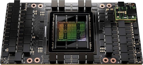
NVIDIA H100 SXM
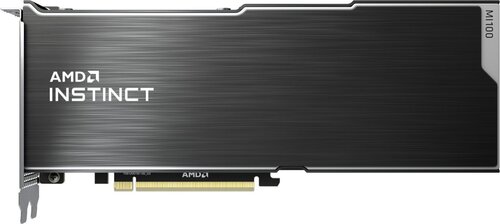
AMD Instinct MI100
|
16896 Shaders
96GB HBM3
1980MHz
|
7680 Shaders
32GB HBM2
1502MHz
|
|
Peak AI Performance
3.96 POPS
INT8 Tensor Sparse
|
Peak AI Performance
184.57 TFLOPS
FP16 Tensor (FP16 Accumulate)
|
|
FP32
66.91 TFLOPS
|
FP32
23.07 TFLOPS
|
|
FP16
133.82 TFLOPS
|
FP16
46.14 TFLOPS
|
|
Form Factor
SXM5
-
|
Form Factor
PCIe Card
2.0-Slots
|
|
TDP
700W
|
TDP
300W
|
|
-
-
-
-
-
|
Power Connectors
-
2x 8-Pin
-
-
|
|
GB6 OpenCL N/A
0%
|
|
|
GB6 Metal N/A
0%
|
GB6 Metal N/A
0%
|
|
GB6 Vulkan N/A
0%
|
GB6 Vulkan N/A
0%
|
|
GB5 OpenCL N/A
0%
|
GB5 OpenCL N/A
0%
|
|
GB5 CUDA N/A
0%
|
GB5 CUDA N/A
0%
|
|
GB5 Metal N/A
0%
|
GB5 Metal N/A
0%
|
|
GB5 Vulkan N/A
0%
|
GB5 Vulkan N/A
0%
|
|
OCT 2020.1 N/A
0%
|
OCT 2020.1 N/A
0%
|
|
OCT Metal N/A
0%
|
OCT Metal N/A
0%
|
|
Peak AI
Performance
3.96 POPS
INT8 Tensor Sparse
|
Peak AI
Performance
184.57 TFLOPS
FP16 Tensor (FP16 Accumulate)
|
|
-
-
-
|
-
-
-
|
|
FP8
-
1.98 PFLOPS
Tensor (FP16 Accumulate)
3.96 PFLOPS
Tensor (FP16 Accumulate) Sparse
1.98 PFLOPS
Tensor (FP32 Accumulate)
3.96 PFLOPS
Tensor (FP32 Accumulate) Sparse
|
-
-
-
-
-
-
|
|
FP16
133.82 TFLOPS
989.43 TFLOPS
Tensor (FP16 Accumulate)
1.98 PFLOPS
Tensor (FP16 Accumulate) Sparse
989.43 TFLOPS
Tensor (FP32 Accumulate)
1.98 PFLOPS
Tensor (FP32 Accumulate) Sparse
|
FP16
46.14 TFLOPS
184.57 TFLOPS
Tensor (FP16 Accumulate)
-
184.57 TFLOPS
Tensor (FP32 Accumulate)
-
|
|
FP32
66.91 TFLOPS
-
-
|
FP32
23.07 TFLOPS
46.14 TFLOPS
Tensor
-
|
|
FP64
33.45 TFLOPS
61.84 TFLOPS
Tensor
|
FP64
11.54 TFLOPS
-
|
|
BF16
133.82 TFLOPS
989.43 TFLOPS
Tensor
1.98 PFLOPS
Tensor Sparse
|
BF16
-
92.28 TFLOPS
Tensor
-
|
|
TF32
494.72 TFLOPS
Tensor
989.43 TFLOPS
Tensor Sparse
|
-
-
-
|
|
-
-
-
|
INT4
92.28 TOPS
Tensor
-
|
|
INT8
-
1.98 POPS
Tensor
3.96 POPS
Tensor Sparse
|
INT8
-
92.28 TOPS
Tensor
-
|
|
INT32
33.45 TOPS
|
-
-
|
|
-
-
|
-
-
|
|
Pixel
Fillrate
47.52 GPixel/s
|
Pixel
Fillrate
-
|
|
-
-
|
-
-
|
|
Texture
Fillrate
1045.44 GTexel/s
|
Texture
Fillrate
720.96 GTexel/s
|
|
Manufacturer
NVIDIA
|
Manufacturer
AMD
|
|
Chip Designer
NVIDIA
|
Chip Designer
AMD
|
|
Architecture
Hopper
|
Architecture
CDNA 1
|
|
Family
Server
|
Family
Instinct
|
|
Codename
NV180
GH100
-
-
|
Codename
Arcturus
-
Variant
Arcturus XL
|
|
Market Segment
Server
|
Market Segment
Server
|
|
Release Date
3/22/2022
|
Release Date
11/16/2020
|
|
Foundry
TSMC
-
|
Foundry
TSMC
-
|
|
Fabrication Node
4N
-
|
Fabrication Node
N7
-
|
|
Die Size
814 mm²
-
|
Die Size
750 mm²
-
|
|
Transistor Count
80 Billion
-
|
Transistor Count
25.6 Billion
-
|
|
Transistor Density
98.28M/mm²
-
|
Transistor Density
34.13M/mm²
-
|
|
Form
SXM5
|
Form
PCIe Card
|
|
Shading Units
16896 Shaders
-
|
Shading Units
7680 Shaders
-
|
|
Texture Mapping Units
528 TMUs
|
Texture Mapping Units
480 TMUs
|
|
Render Output Units
24 ROPs
|
Render Output Units
-
|
|
Tensor Cores
528 T-Cores
|
Tensor Cores
480 T-Cores
|
|
-
-
|
-
-
|
|
Streaming Multiprocessors
132 SMs
|
-
-
|
|
-
-
|
Compute Units
120 CUs
|
|
-
-
|
-
-
|
|
-
-
|
-
-
|
|
1830MHz Tensor
-
1065MHz Base
1980MHz
|
-
-
1000MHz Base
1502MHz
|
|
-
-
|
-
-
|
|
L1
64KB/SM Tex
256KB/SM
-
-
|
L1
-
-
16KB/CU
-
|
|
L2
50MB Shared
|
L2
8MB Shared
|
|
-
-
-
|
-
-
-
|
|
96GB
HBM3
-
|
32GB
HBM2
ECC
|
|
Bus Width
5120Bit
|
Bus Width
4096Bit
|
|
Clock
2619MHz
Transfer Rate
5.2GT/s
Bandwidth
3352.3GB/s
|
Clock
1200MHz
Transfer Rate
2.4GT/s
Bandwidth
1228.8GB/s
|
|
-
-
-
-
-
-
-
-
-
|
-
-
-
-
-
-
-
-
-
|
|
TDP
700W
|
TDP
300W
|
|
-
-
|
-
-
|
|
-
-
-
-
-
-
-
-
-
-
-
-
-
-
-
-
-
-
-
-
-
-
-
-
-
-
-
-
-
-
-
-
-
-
-
-
-
-
-
No Ports
|
-
-
-
-
-
-
-
-
-
-
-
-
-
-
-
-
-
-
-
-
-
-
-
-
-
-
-
-
-
-
-
-
-
-
-
-
-
-
-
No Ports
|
|
Max Resolution
Unknown
|
Max Resolution
Unknown
|
|
Max Resolution Refresh Rate
-
|
Max Resolution Refresh Rate
-
|
|
Variable Refresh Rate
G-Sync
FreeSync
-
|
Variable Refresh Rate
-
-
-
|
|
Display Stream Compression (DSC)
Not Supported
|
Display Stream Compression (DSC)
Not Supported
|
|
Multi Monitor Support
Unknown
|
Multi Monitor Support
Unknown
|
|
-
-
|
-
-
|
|
No Encoders
-
|
Model
VCN 2.5
|
|
-
-
-
-
-
-
-
-
-
-
-
-
-
-
-
|
Codec
-
-
-
-
-
-
-
-
AVC (H.264)
HEVC (H.265)
-
-
-
-
|
|
Model
7x NVDEC 5
|
Model
VCN 2.5
|
|
Codec
MPEG-1
MPEG-2
MPEG-4
-
VC-1
VP8
VP9
-
AVC (H.264)
HEVC (H.265)
-
AV1
-
-
|
Codec
MPEG-1
MPEG-2
MPEG-4
JPEG
VC-1
-
VP9
-
AVC (H.264)
HEVC (H.265)
-
-
-
-
|
|
-
-
-
-
|
-
-
-
-
|
|
-
-
OpenCL
3.0
-
-
|
-
-
OpenCL
2.1
-
-
|
|
-
-
CUDA
9.0
-
-
PureVideo HD
VP11
VDPAU
Feature Set K
|
-
-
-
-
GFX
9.4
-
-
-
-
|
|
Not a Card
-
-
-
|
-
-
-
-
|
|
-
-
-
-
-
-
-
-
|
Power Connectors
-
-
-
2x 8-Pin
-
-
-
|
|
-
-
PCIe Version
5.0
PCIe Lanes
16
|
Slots Required
2.0
PCIe Version
4.0
PCIe Lanes
16
|
|
Multi GPU Support
Supported
Type
NVLink
|
Multi GPU Support
Supported
Type
Infinity Fabric
|
|
-
-
-
-
-
-
|
Height
111 mm (4.37 in)
Width
267 mm (10.51 in)
Depth
37 mm (1.46 in)
|


Copy Link