NVIDIA H100 vs NVIDIA A100 SXM 40GB
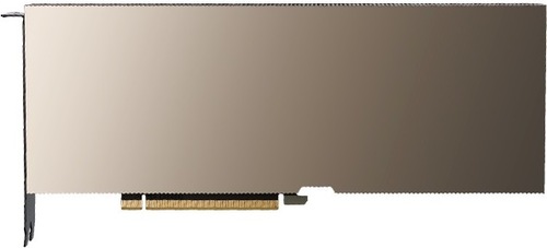
NVIDIA H100
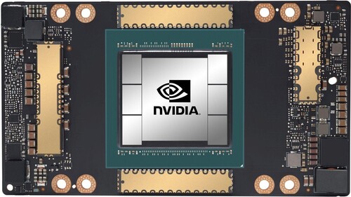
NVIDIA A100 SXM 40GB
|
14592 Shaders
80GB HBM2e
1755MHz
|
6912 Shaders
40GB HBM2e
1410MHz
|
|
Peak AI Performance
3.03 POPS
INT8 Tensor Sparse
|
Peak AI Performance
2.49 POPS
INT4 Tensor Sparse
|
|
FP32
51.22 TFLOPS
|
FP32
19.49 TFLOPS
|
|
FP16
102.44 TFLOPS
|
FP16
77.97 TFLOPS
|
|
Form Factor
PCIe Card
2.0-Slots
|
Form Factor
SXM4
-
|
|
TDP
350W
|
TDP
400W
|
|
Power Connectors
-
-
-
1x 16-Pin 12VHPWR
|
-
-
-
-
-
|
|
GB6 OpenCL N/A
0%
|
|
|
GB6 Metal N/A
0%
|
GB6 Metal N/A
0%
|
|
GB6 Vulkan N/A
0%
|
|
GB5 OpenCL N/A
0%
|
GB5 OpenCL N/A
0%
|
|
GB5 CUDA N/A
0%
|
GB5 CUDA N/A
0%
|
|
GB5 Metal N/A
0%
|
GB5 Metal N/A
0%
|
|
GB5 Vulkan N/A
0%
|
GB5 Vulkan N/A
0%
|
|
OCT 2020.1 N/A
0%
|
OCT 2020.1 N/A
0%
|
|
OCT Metal N/A
0%
|
OCT Metal N/A
0%
|
|
Peak AI
Performance
3.03 POPS
INT8 Tensor Sparse
|
Peak AI
Performance
2.49 POPS
INT4 Tensor Sparse
|
|
-
-
-
|
-
-
-
|
|
FP8
-
1.51 PFLOPS
Tensor (FP16 Accumulate)
3.03 PFLOPS
Tensor (FP16 Accumulate) Sparse
1.51 PFLOPS
Tensor (FP32 Accumulate)
3.03 PFLOPS
Tensor (FP32 Accumulate) Sparse
|
-
-
-
-
-
-
|
|
FP16
102.44 TFLOPS
756.45 TFLOPS
Tensor (FP16 Accumulate)
1.51 PFLOPS
Tensor (FP16 Accumulate) Sparse
756.45 TFLOPS
Tensor (FP32 Accumulate)
1.51 PFLOPS
Tensor (FP32 Accumulate) Sparse
|
FP16
77.97 TFLOPS
311.87 TFLOPS
Tensor (FP16 Accumulate)
623.74 TFLOPS
Tensor (FP16 Accumulate) Sparse
311.87 TFLOPS
Tensor (FP32 Accumulate)
623.74 TFLOPS
Tensor (FP32 Accumulate) Sparse
|
|
FP32
51.22 TFLOPS
-
-
|
FP32
19.49 TFLOPS
-
-
|
|
FP64
25.61 TFLOPS
47.28 TFLOPS
Tensor
|
FP64
9.75 TFLOPS
19.49 TFLOPS
Tensor
|
|
BF16
102.44 TFLOPS
756.45 TFLOPS
Tensor
1.51 PFLOPS
Tensor Sparse
|
BF16
38.98 TFLOPS
311.87 TFLOPS
Tensor
623.74 TFLOPS
Tensor Sparse
|
|
TF32
378.23 TFLOPS
Tensor
756.45 TFLOPS
Tensor Sparse
|
TF32
155.94 TFLOPS
Tensor
311.87 TFLOPS
Tensor Sparse
|
|
-
-
-
|
INT4
1.25 POPS
Tensor
2.49 POPS
Tensor Sparse
|
|
INT8
-
1.51 POPS
Tensor
3.03 POPS
Tensor Sparse
|
INT8
-
623.74 TOPS
Tensor
1.25 POPS
Tensor Sparse
|
|
INT32
25.61 TOPS
|
INT32
19.49 TOPS
|
|
-
-
|
-
-
|
|
Pixel
Fillrate
42.12 GPixel/s
|
Pixel
Fillrate
225.6 GPixel/s
|
|
-
-
|
-
-
|
|
Texture
Fillrate
800.28 GTexel/s
|
Texture
Fillrate
609.12 GTexel/s
|
|
Foundry
TSMC
-
|
Foundry
TSMC
-
|
|
Fabrication Node
4N
-
|
Fabrication Node
7N
-
|
|
Die Size
814 mm²
-
|
Die Size
826 mm²
-
|
|
Transistor Count
80 Billion
-
|
Transistor Count
54.2 Billion
-
|
|
Transistor Density
98.28M/mm²
-
|
Transistor Density
65.62M/mm²
-
|
|
Form
PCIe Card
|
Form
SXM4
|
|
Shading Units
14592 Shaders
-
|
Shading Units
6912 Shaders
-
|
|
Texture Mapping Units
456 TMUs
|
Texture Mapping Units
432 TMUs
|
|
Render Output Units
24 ROPs
|
Render Output Units
160 ROPs
|
|
Tensor Cores
456 T-Cores
|
Tensor Cores
432 T-Cores
|
|
-
-
|
-
-
|
|
Streaming Multiprocessors
114 SMs
|
Streaming Multiprocessors
108 SMs
|
|
-
-
|
-
-
|
|
-
-
|
-
-
|
|
-
-
|
-
-
|
|
1620MHz Tensor
-
1065MHz Base
1755MHz
|
-
-
1095MHz Base
1410MHz
|
|
-
-
|
-
-
|
|
L1
64KB/SM Tex
256KB/SM
-
-
|
L1
64KB/SM Tex
192KB/SM
-
-
|
|
L2
50MB Shared
|
L2
40MB Shared
|
|
-
-
-
|
-
-
-
|
|
80GB
HBM2e
-
|
40GB
HBM2e
-
|
|
Bus Width
5120Bit
|
Bus Width
5120Bit
|
|
Clock
1593MHz
Transfer Rate
3.2GT/s
Bandwidth
2039GB/s
|
Clock
1215MHz
Transfer Rate
2.4GT/s
Bandwidth
1555.2GB/s
|
|
-
-
-
-
-
-
-
-
-
|
-
-
-
-
-
-
-
-
-
|
|
TDP
350W
|
TDP
400W
|
|
-
-
|
-
-
|
|
-
-
-
-
-
-
-
-
-
-
-
-
-
-
-
-
-
-
-
-
-
-
-
-
-
-
-
-
-
-
-
-
-
-
-
-
-
-
-
No Ports
|
-
-
-
-
-
-
-
-
-
-
-
-
-
-
-
-
-
-
-
-
-
-
-
-
-
-
-
-
-
-
-
-
-
-
-
-
-
-
-
No Ports
|
|
Max Resolution
Unknown
|
Max Resolution
Unknown
|
|
Max Resolution Refresh Rate
-
|
Max Resolution Refresh Rate
-
|
|
Variable Refresh Rate
G-Sync
FreeSync
-
|
Variable Refresh Rate
G-Sync
FreeSync
-
|
|
Display Stream Compression (DSC)
Not Supported
|
Display Stream Compression (DSC)
Not Supported
|
|
Multi Monitor Support
Unknown
|
Multi Monitor Support
Unknown
|
|
-
-
|
-
-
|
|
No Encoders
-
|
No Encoders
-
|
|
-
-
-
-
-
-
-
-
-
-
-
-
-
-
-
|
-
-
-
-
-
-
-
-
-
-
-
-
-
-
-
|
|
Model
7x NVDEC 5
|
Model
5x NVDEC 4
|
|
Codec
MPEG-1
MPEG-2
MPEG-4
-
VC-1
VP8
VP9
-
AVC (H.264)
HEVC (H.265)
-
AV1
-
-
|
Codec
MPEG-1
MPEG-2
MPEG-4
-
VC-1
VP8
VP9
-
AVC (H.264)
HEVC (H.265)
-
-
-
-
|
|
-
-
-
-
|
-
-
-
-
|
|
-
-
OpenCL
3.0
-
-
|
-
-
OpenCL
3.0
Vulkan
1.2
|
|
-
-
CUDA
9.0
-
-
PureVideo HD
VP11
VDPAU
Feature Set K
|
-
-
CUDA
8.0
-
-
PureVideo HD
VP10
VDPAU
Feature Set J
|
|
-
-
-
-
|
Not a Card
-
-
-
|
|
Power Connectors
-
-
-
-
-
-
1x 16-Pin 12VHPWR
|
-
-
-
-
-
-
-
-
|
|
Slots Required
2.0
PCIe Version
5.0
PCIe Lanes
16
|
-
-
PCIe Version
4.0
PCIe Lanes
16
|
|
Multi GPU Support
Supported
Type
NVLink
|
Multi GPU Support
Supported
Type
NVLink
|
|
Height
111 mm (4.37 in)
Width
268 mm (10.55 in)
Depth
40 mm (1.57 in)
|
-
-
-
-
-
-
|


Copy Link