NVIDIA L40S vs NVIDIA T40
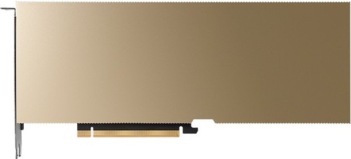
NVIDIA L40S

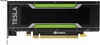
NVIDIA T40
|
18176 Shaders
48GB GDDR6
2520MHz
|
4608 Shaders
24GB GDDR6
1560MHz
|
|
Peak AI Performance
2.93 POPS
INT4 Tensor Sparse
|
Peak AI Performance
460.06 TOPS
INT4 Tensor
|
|
FP32
91.61 TFLOPS
|
FP32
14.38 TFLOPS
|
|
FP16
91.61 TFLOPS
|
FP16
28.75 TFLOPS
|
|
Form Factor
PCIe Card
2.0-Slots
|
Form Factor
PCIe Card
1.0-Slots
|
|
TDP
300W
|
TDP
150W
|
|
Power Connectors
-
-
-
1x 16-Pin 12VHPWR
|
Power Connectors
1x 6-Pin
1x 8-Pin
-
-
|
|
GB6 OpenCL N/A
0%
|
|
|
GB6 Metal N/A
0%
|
GB6 Metal N/A
0%
|
|
GB6 Vulkan N/A
0%
|
|
GB5 OpenCL N/A
0%
|
GB5 OpenCL N/A
0%
|
|
GB5 CUDA N/A
0%
|
GB5 CUDA N/A
0%
|
|
GB5 Metal N/A
0%
|
GB5 Metal N/A
0%
|
|
GB5 Vulkan N/A
0%
|
GB5 Vulkan N/A
0%
|
|
OCT 2020.1 N/A
0%
|
OCT 2020.1 N/A
0%
|
|
OCT Metal N/A
0%
|
OCT Metal N/A
0%
|
|
Peak AI
Performance
2.93 POPS
INT4 Tensor Sparse
|
Peak AI
Performance
460.06 TOPS
INT4 Tensor
|
|
-
-
-
|
-
-
-
|
|
FP8
-
732.86 TFLOPS
Tensor (FP16 Accumulate)
1.47 PFLOPS
Tensor (FP16 Accumulate) Sparse
732.86 TFLOPS
Tensor (FP32 Accumulate)
1.47 PFLOPS
Tensor (FP32 Accumulate) Sparse
|
-
-
-
-
-
-
|
|
FP16
91.61 TFLOPS
366.43 TFLOPS
Tensor (FP16 Accumulate)
732.86 TFLOPS
Tensor (FP16 Accumulate) Sparse
366.43 TFLOPS
Tensor (FP32 Accumulate)
732.86 TFLOPS
Tensor (FP32 Accumulate) Sparse
|
FP16
28.75 TFLOPS
115.02 TFLOPS
Tensor (FP16 Accumulate)
-
115.02 TFLOPS
Tensor (FP32 Accumulate)
-
|
|
FP32
91.61 TFLOPS
-
-
|
FP32
14.38 TFLOPS
-
-
|
|
FP64
1.43 TFLOPS
-
|
FP64
450 GFLOPS
-
|
|
BF16
91.61 TFLOPS
366.43 TFLOPS
Tensor
732.86 TFLOPS
Tensor Sparse
|
-
-
-
-
|
|
TF32
183.21 TFLOPS
Tensor
366.43 TFLOPS
Tensor Sparse
|
-
-
-
|
|
INT4
1.47 POPS
Tensor
2.93 POPS
Tensor Sparse
|
INT4
460.06 TOPS
Tensor
-
|
|
INT8
-
732.86 TOPS
Tensor
1.47 POPS
Tensor Sparse
|
INT8
-
230.03 TOPS
Tensor
-
|
|
INT32
45.8 TOPS
|
-
-
|
|
Ray Tracing
211.7 TOPS
|
Ray Tracing
56.2 TOPS
|
|
Pixel
Fillrate
483.84 GPixel/s
|
Pixel
Fillrate
149.76 GPixel/s
|
|
-
-
|
-
-
|
|
Texture
Fillrate
1431.36 GTexel/s
|
Texture
Fillrate
449.28 GTexel/s
|
|
Manufacturer
NVIDIA
|
Manufacturer
NVIDIA
|
|
Chip Designer
NVIDIA
|
Chip Designer
NVIDIA
|
|
Architecture
Ada Lovelace
|
Architecture
Turing
|
|
Family
Server
|
Family
Server
|
|
Codename
NV182
AD102
Variant
AD102-895-A1
|
Codename
NV162
TU102
Variant
TU102-890-KCD-A1
|
|
Market Segment
Server
|
Market Segment
Server
|
|
Release Date
10/13/2022
|
Release Date
9/13/2018
|
|
Foundry
TSMC
-
|
Foundry
TSMC
-
|
|
Fabrication Node
4N
-
|
Fabrication Node
12FFN
-
|
|
Die Size
608 mm²
-
|
Die Size
754 mm²
-
|
|
Transistor Count
76.3 Billion
-
|
Transistor Count
18.6 Billion
-
|
|
Transistor Density
125.41M/mm²
-
|
Transistor Density
24.67M/mm²
-
|
|
Form
PCIe Card
|
Form
PCIe Card
|
|
Shading Units
18176 Shaders
-
|
Shading Units
4608 Shaders
-
|
|
Texture Mapping Units
568 TMUs
|
Texture Mapping Units
288 TMUs
|
|
Render Output Units
192 ROPs
|
Render Output Units
96 ROPs
|
|
Tensor Cores
568 T-Cores
|
Tensor Cores
576 T-Cores
|
|
Ray-Tracing Cores
142 RT-Cores
|
Ray-Tracing Cores
72 RT-Cores
|
|
Streaming Multiprocessors
142 SMs
|
Streaming Multiprocessors
72 SMs
|
|
-
-
|
-
-
|
|
-
-
|
-
-
|
|
Graphics Processing Clusters
12 GPCs
|
-
-
|
|
-
-
1110MHz Base
2520MHz
|
-
-
1305MHz Base
1560MHz
|
|
-
-
|
-
-
|
|
L1
64KB/SM Tex
128KB/SM
-
-
|
L1
32KB/SM Tex
64KB/SM
-
-
|
|
L2
96MB Shared
|
L2
6MB Shared
|
|
-
-
-
|
-
-
-
|
|
48GB
GDDR6
-
|
24GB
GDDR6
-
|
|
Bus Width
384Bit
|
Bus Width
384Bit
|
|
Clock
2250MHz
Transfer Rate
18GT/s
Bandwidth
864GB/s
|
Clock
1625MHz
Transfer Rate
13GT/s
Bandwidth
624GB/s
|
|
-
-
-
-
-
-
-
-
-
|
-
-
-
-
-
-
-
-
-
|
|
TDP
300W
|
TDP
150W
|
|
-
-
|
-
-
|
|
-
-
-
-
-
-
-
-
-
-
-
-
-
-
-
-
-
-
-
-
-
-
-
-
4x DisplayPort 1.4
-
-
-
-
-
-
-
-
-
-
-
-
-
-
|
-
-
-
-
-
-
-
-
-
-
-
-
-
-
-
-
-
-
-
-
-
-
-
-
-
-
-
-
-
-
-
-
-
-
-
-
-
-
-
No Ports
|
|
Max Resolution
7680x4320
|
Max Resolution
Unknown
|
|
Max Resolution Refresh Rate
120Hz
|
Max Resolution Refresh Rate
-
|
|
Variable Refresh Rate
G-Sync
FreeSync
-
|
Variable Refresh Rate
G-Sync
FreeSync
-
|
|
Display Stream Compression (DSC)
Supported
|
Display Stream Compression (DSC)
Not Supported
|
|
Multi Monitor Support
4
|
Multi Monitor Support
Unknown
|
|
Content Protection
HDCP 2.3
|
-
-
|
|
Model
2x NVENC 8
|
Model
NVENC 7
|
|
Codec
-
-
-
-
-
-
-
-
AVC (H.264)
HEVC (H.265)
-
AV1
-
-
|
Codec
-
-
-
-
-
-
-
-
AVC (H.264)
HEVC (H.265)
-
-
-
-
|
|
Model
NVDEC 5
|
Model
NVDEC 4
|
|
Codec
MPEG-1
MPEG-2
MPEG-4
-
VC-1
VP8
VP9
-
AVC (H.264)
HEVC (H.265)
-
AV1
-
-
|
Codec
MPEG-1
MPEG-2
MPEG-4
-
VC-1
VP8
VP9
-
AVC (H.264)
HEVC (H.265)
-
-
-
-
|
|
Direct X
12
Direct 3D
12_3
|
Direct X
12
Direct 3D
12_2
|
|
OpenGL
4.6
OpenCL
3.0
Vulkan
1.3
|
OpenGL
4.6
OpenCL
3.0
Vulkan
1.2
|
|
Shader Model
6.7
CUDA
8.9
-
-
PureVideo HD
VP12
VDPAU
Feature Set L
|
Shader Model
6.6
CUDA
7.5
-
-
PureVideo HD
VP10
VDPAU
Feature Set J
|
|
-
-
-
-
|
-
-
-
-
|
|
Power Connectors
-
-
-
-
-
-
1x 16-Pin 12VHPWR
|
Power Connectors
-
-
1x 6-Pin
1x 8-Pin
-
-
-
|
|
Slots Required
2.0
PCIe Version
4.0
PCIe Lanes
16
|
Slots Required
1.0
PCIe Version
3.0
PCIe Lanes
16
|
|
-
-
-
-
|
Multi GPU Support
Supported
Type
NVLink
|
|
Height
111 mm (4.37 in)
Width
267 mm (10.51 in)
Depth
40 mm (1.57 in)
|
Height
111 mm (4.37 in)
Width
267 mm (10.51 in)
Depth
20 mm (0.79 in)
|


Copy Link