NVIDIA Quadro T1000 vs AMD Radeon PRO W5700
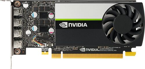
NVIDIA Quadro T1000
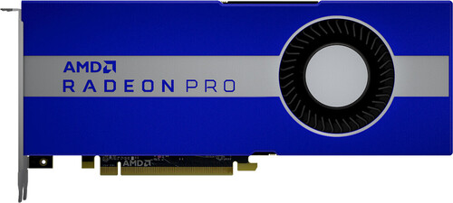
AMD Radeon PRO W5700
$799
|
896 Shaders
4GB GDDR6
1400MHz
|
2304 Shaders
8GB GDDR6
1880MHz
|
|
Peak AI Performance
5.02 TFLOPS
FP16
|
Peak AI Performance
17.33 TFLOPS
FP16
|
|
FP32
2.51 TFLOPS
|
FP32
8.66 TFLOPS
|
|
FP16
5.02 TFLOPS
|
FP16
17.33 TFLOPS
|
|
Form Factor
PCIe Card
1.0-Slots
|
Form Factor
PCIe Card
2.0-Slots
|
|
TDP
50W
|
TDP
205W
|
|
-
-
-
-
-
|
-
-
-
-
-
|
|
GB6 Metal N/A
0%
|
GB6 Metal 87,840
35%
|
|
GB6 Vulkan N/A
0%
|
|
GB5 OpenCL N/A
0%
|
GB5 OpenCL N/A
0%
|
|
GB5 CUDA N/A
0%
|
GB5 CUDA N/A
0%
|
|
GB5 Metal N/A
0%
|
GB5 Metal N/A
0%
|
|
GB5 Vulkan N/A
0%
|
GB5 Vulkan N/A
0%
|
|
OCT 2020.1 N/A
0%
|
OCT 2020.1 N/A
0%
|
|
OCT Metal N/A
0%
|
OCT Metal N/A
0%
|
|
Peak AI
Performance
5.02 TFLOPS
FP16
|
Peak AI
Performance
17.33 TFLOPS
FP16
|
|
-
-
-
|
-
-
-
|
|
-
-
-
-
-
-
|
-
-
-
-
-
-
|
|
FP16
5.02 TFLOPS
-
-
-
-
|
FP16
17.33 TFLOPS
-
-
-
-
|
|
FP32
2.51 TFLOPS
-
-
|
FP32
8.66 TFLOPS
-
-
|
|
FP64
80 GFLOPS
-
|
FP64
540 GFLOPS
-
|
|
-
-
-
-
|
-
-
-
-
|
|
-
-
-
|
-
-
-
|
|
-
-
-
|
-
-
-
|
|
-
-
-
-
|
-
-
-
-
|
|
-
-
|
-
-
|
|
-
-
|
-
-
|
|
Pixel
Fillrate
44.8 GPixel/s
|
Pixel
Fillrate
120.32 GPixel/s
|
|
-
-
|
-
-
|
|
Texture
Fillrate
78.4 GTexel/s
|
Texture
Fillrate
270.72 GTexel/s
|
|
Manufacturer
NVIDIA
|
Manufacturer
AMD
|
|
Chip Designer
NVIDIA
|
Chip Designer
AMD
|
|
Architecture
Turing
|
Architecture
RDNA 1
|
|
Family
Quadro T
|
Family
Radeon PRO W
|
|
Codename
NV167
TU117
-
-
|
Codename
Gaming
Navi 10
Variant
Navi 10 XL GL
|
|
Market Segment
Workstation
|
Market Segment
Workstation
|
|
Release Date
5/6/2021
|
Release Date
11/19/2019
|
|
Foundry
TSMC
-
|
Foundry
TSMC
-
|
|
Fabrication Node
12FFN
-
|
Fabrication Node
N7
-
|
|
Die Size
200 mm²
-
|
Die Size
251 mm²
-
|
|
Transistor Count
4.7 Billion
-
|
Transistor Count
10.3 Billion
-
|
|
Transistor Density
23.50M/mm²
-
|
Transistor Density
41.04M/mm²
-
|
|
Form
PCIe Card
|
Form
PCIe Card
|
|
Shading Units
896 Shaders
-
|
Shading Units
2304 Shaders
-
|
|
Texture Mapping Units
56 TMUs
|
Texture Mapping Units
144 TMUs
|
|
Render Output Units
32 ROPs
|
Render Output Units
64 ROPs
|
|
-
-
|
-
-
|
|
-
-
|
-
-
|
|
Streaming Multiprocessors
14 SMs
|
-
-
|
|
-
-
|
Compute Units
36 CUs
|
|
-
-
|
-
-
|
|
-
-
|
-
-
|
|
-
-
-
1400MHz
|
-
-
1400MHz Base
1880MHz
|
|
-
-
|
L0
32KB/WGP
|
|
L1
32KB/SM Tex
64KB/SM
-
-
|
L1
-
-
-
128KB/Array
|
|
L2
1MB Shared
|
L2
4MB Shared
|
|
-
-
-
|
-
-
-
|
|
4GB
GDDR6
-
|
8GB
GDDR6
-
|
|
Bus Width
128Bit
|
Bus Width
256Bit
|
|
Clock
1250MHz
Transfer Rate
10GT/s
Bandwidth
160GB/s
|
Clock
1750MHz
Transfer Rate
14GT/s
Bandwidth
448GB/s
|
|
-
-
-
-
-
-
-
-
-
|
-
-
-
-
-
-
-
-
-
|
|
TDP
50W
|
TDP
205W
|
|
-
-
|
-
-
|
|
-
-
-
-
-
-
-
-
-
-
-
-
-
-
-
-
-
4x mini-DisplayPort 1.4
-
-
-
-
-
-
-
-
-
-
-
-
-
-
-
-
-
-
-
-
-
|
-
-
-
-
-
-
-
-
-
-
-
-
-
-
-
-
-
5x mini-DisplayPort 1.4
-
-
-
-
-
-
-
-
-
-
-
-
-
-
-
-
-
-
-
1x USB-C + DP
-
|
|
Max Resolution
7680x4320
|
Max Resolution
7680x4320
|
|
Max Resolution Refresh Rate
120Hz
|
Max Resolution Refresh Rate
120Hz
|
|
Variable Refresh Rate
G-Sync
FreeSync
-
|
Variable Refresh Rate
-
FreeSync
-
|
|
Display Stream Compression (DSC)
Supported
|
Display Stream Compression (DSC)
Supported
|
|
Multi Monitor Support
4
|
Multi Monitor Support
4
|
|
Content Protection
HDCP 2.2
|
Content Protection
HDCP 2.3
|
|
Model
NVENC 7
|
Model
VCN 2.0
|
|
Codec
-
-
-
-
-
-
-
-
AVC (H.264)
HEVC (H.265)
-
-
-
-
|
Codec
-
-
-
-
-
-
-
-
AVC (H.264)
HEVC (H.265)
-
-
-
-
|
|
Model
NVDEC 4
|
Model
VCN 2.0
|
|
Codec
MPEG-1
MPEG-2
MPEG-4
-
VC-1
VP8
VP9
-
AVC (H.264)
HEVC (H.265)
-
-
-
-
|
Codec
MPEG-1
MPEG-2
MPEG-4
JPEG
VC-1
-
VP9
-
AVC (H.264)
HEVC (H.265)
-
-
-
-
|
|
Direct X
12
Direct 3D
12_2
|
Direct X
12
Direct 3D
12_1
|
|
OpenGL
4.6
OpenCL
3.0
Vulkan
1.2
|
OpenGL
4.6
OpenCL
2.1
Vulkan
1.2
|
|
Shader Model
6.6
CUDA
7.5
-
-
PureVideo HD
VP10
VDPAU
Feature Set J
|
Shader Model
6.5
-
-
GFX
10.1
-
-
-
-
|
|
-
-
-
1x Fan
|
-
-
-
1x Fan
|
|
-
-
-
-
-
-
-
-
|
-
-
-
-
-
-
-
-
|
|
Slots Required
1.0
PCIe Version
3.0
PCIe Lanes
16
|
Slots Required
2.0
PCIe Version
4.0
PCIe Lanes
16
|
|
-
-
-
-
|
Multi GPU Support
Supported
Type
CrossFire XDMA
|
|
Height
69 mm (2.72 in)
Width
150 mm (5.91 in)
Depth
20 mm (0.79 in)
|
Height
111 mm (4.37 in)
Width
267 mm (10.51 in)
Depth
37 mm (1.46 in)
|


Copy Link