NVIDIA RTX A1000 vs AMD Radeon PRO W7800

NVIDIA RTX A1000
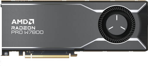
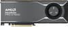
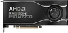
AMD Radeon PRO W7800
$2,499
|
2307 Shaders
8GB GDDR6
1462MHz
|
4480 Shaders
32GB GDDR6
2525MHz
|
|
Peak AI Performance
215.58 TOPS
INT4 Tensor Sparse
|
Peak AI Performance
180.99 TOPS
INT4 Tensor
|
|
FP32
6.75 TFLOPS
|
FP32
45.25 TFLOPS
|
|
FP16
6.75 TFLOPS
|
FP16
90.5 TFLOPS
|
|
Form Factor
PCIe Card
1.0-Slots
|
Form Factor
PCIe Card
2.0-Slots
|
|
TDP
50W
|
TDP
260W
|
|
-
-
-
-
-
|
Power Connectors
-
2x 8-Pin
-
-
|
|
GB6 OpenCL N/A
0%
|
|
|
GB6 Metal N/A
0%
|
GB6 Metal N/A
0%
|
|
GB5 OpenCL N/A
0%
|
GB5 OpenCL N/A
0%
|
|
GB5 CUDA N/A
0%
|
GB5 CUDA N/A
0%
|
|
GB5 Metal N/A
0%
|
GB5 Metal N/A
0%
|
|
GB5 Vulkan N/A
0%
|
GB5 Vulkan N/A
0%
|
|
OCT 2020.1 N/A
0%
|
OCT 2020.1 N/A
0%
|
|
OCT Metal N/A
0%
|
OCT Metal N/A
0%
|
|
Peak AI
Performance
215.58 TOPS
INT4 Tensor Sparse
|
Peak AI
Performance
180.99 TOPS
INT4 Tensor
|
|
-
-
-
|
-
-
-
|
|
-
-
-
-
-
-
|
-
-
-
-
-
-
|
|
FP16
6.75 TFLOPS
26.95 TFLOPS
Tensor (FP16 Accumulate)
53.9 TFLOPS
Tensor (FP16 Accumulate) Sparse
26.95 TFLOPS
Tensor (FP32 Accumulate)
53.9 TFLOPS
Tensor (FP32 Accumulate) Sparse
|
FP16
90.5 TFLOPS
45.25 TFLOPS
Tensor (FP16 Accumulate)
-
45.25 TFLOPS
Tensor (FP32 Accumulate)
-
|
|
FP32
6.75 TFLOPS
-
-
|
FP32
45.25 TFLOPS
-
-
|
|
FP64
110 GFLOPS
-
|
FP64
1.41 TFLOPS
-
|
|
BF16
6.75 TFLOPS
26.95 TFLOPS
Tensor
53.9 TFLOPS
Tensor Sparse
|
BF16
90.5 TFLOPS
45.25 TFLOPS
Tensor
-
|
|
TF32
13.47 TFLOPS
Tensor
26.95 TFLOPS
Tensor Sparse
|
-
-
-
|
|
INT4
107.79 TOPS
Tensor
215.58 TOPS
Tensor Sparse
|
INT4
180.99 TOPS
Tensor
-
|
|
INT8
-
53.9 TOPS
Tensor
107.79 TOPS
Tensor Sparse
|
INT8
-
45.25 TOPS
Tensor
-
|
|
INT32
3.37 TOPS
|
INT32
22.62 TOPS
|
|
Ray Tracing
13.2 TOPS
|
-
-
|
|
Pixel
Fillrate
70.176 GPixel/s
|
Pixel
Fillrate
323.2 GPixel/s
|
|
-
-
|
-
-
|
|
Texture
Fillrate
105.264 GTexel/s
|
Texture
Fillrate
707 GTexel/s
|
|
Manufacturer
NVIDIA
|
Manufacturer
AMD
|
|
Chip Designer
NVIDIA
|
Chip Designer
AMD
|
|
Architecture
Ampere
|
Architecture
RDNA 3
|
|
Family
RTX A
|
Family
Radeon PRO W
|
|
Codename
NV177
GA107
-
-
|
Codename
Plum Bonito
Navi 31
Variant
Navi 31 XL GL
|
|
Market Segment
Workstation
|
Market Segment
Workstation
|
|
Release Date
4/17/2023
|
Release Date
4/13/2023
|
|
Foundry
Samsung
-
|
Foundry
TSMC
TSMC Memory Cache Die
|
|
Fabrication Node
8N
-
|
Fabrication Node
N5
N6 Memory Cache Die
|
|
Die Size
200 mm²
-
|
Die Size
304 mm²
6x 38 mm² Memory Cache Die
|
|
Transistor Count
8.7 Billion
-
|
Transistor Count
45.4 Billion
6x 2.1 Billion Memory Cache Die
|
|
Transistor Density
43.50M/mm²
-
|
Transistor Density
149.17M/mm²
54.64M/mm² Memory Cache Die
|
|
Form
PCIe Card
|
Form
PCIe Card
|
|
Shading Units
2307 Shaders
-
|
Shading Units
4480 Shaders
-
|
|
Texture Mapping Units
72 TMUs
|
Texture Mapping Units
280 TMUs
|
|
Render Output Units
48 ROPs
|
Render Output Units
128 ROPs
|
|
Tensor Cores
72 T-Cores
|
Tensor Cores
140 T-Cores
|
|
Ray-Tracing Cores
18 RT-Cores
|
Ray-Tracing Cores
70 RT-Cores
|
|
Streaming Multiprocessors
18 SMs
|
-
-
|
|
-
-
|
Compute Units
70 CUs
|
|
-
-
|
-
-
|
|
Graphics Processing Clusters
3 GPCs
|
-
-
|
|
-
-
1140MHz Base
1462MHz
|
-
-
-
2525MHz
|
|
-
-
|
L0
64KB/WGP
|
|
L1
64KB/SM Tex
128KB/SM
-
-
|
L1
-
-
-
256KB/Array
|
|
L2
2MB Shared
|
L2
6MB Shared
|
|
-
-
-
|
L3
64MB Shared
2.33TB/s
|
|
8GB
GDDR6
-
|
32GB
GDDR6
-
|
|
Bus Width
128Bit
|
Bus Width
256Bit
|
|
Clock
1500MHz
Transfer Rate
12GT/s
Bandwidth
192GB/s
|
Clock
2250MHz
Transfer Rate
18GT/s
Bandwidth
576GB/s
|
|
-
-
-
-
-
-
-
-
-
|
-
-
-
-
-
-
-
-
-
|
|
TDP
50W
|
TDP
260W
|
|
-
-
|
-
-
|
|
-
-
-
-
-
-
-
-
-
-
-
-
-
-
-
-
-
4x mini-DisplayPort 1.4
-
-
-
-
-
-
-
-
-
-
-
-
-
-
-
-
-
-
-
-
-
|
-
-
-
-
-
-
-
-
-
-
-
-
-
-
-
-
-
-
-
1x mini-DisplayPort 2.1
-
-
-
-
-
-
3x DisplayPort 2.1
-
-
-
-
-
-
-
-
-
-
-
-
|
|
Max Resolution
7680x4320
|
Max Resolution
15360x8640
|
|
Max Resolution Refresh Rate
60Hz
|
Max Resolution Refresh Rate
165Hz
|
|
Variable Refresh Rate
G-Sync
FreeSync
-
|
Variable Refresh Rate
-
FreeSync
-
|
|
Display Stream Compression (DSC)
Supported
|
Display Stream Compression (DSC)
Supported
|
|
Multi Monitor Support
3
|
Multi Monitor Support
3
|
|
Content Protection
HDCP 2.3
|
Content Protection
HDCP 2.3
|
|
Model
NVENC 7
|
Model
VCN 4.0
|
|
Codec
-
-
-
-
-
-
-
-
AVC (H.264)
HEVC (H.265)
-
-
-
-
|
Codec
-
-
-
-
-
-
VP9
-
AVC (H.264)
HEVC (H.265)
-
AV1
-
-
|
|
Model
NVDEC 5
|
Model
VCN 4.0
|
|
Codec
MPEG-1
MPEG-2
MPEG-4
-
VC-1
VP8
VP9
-
AVC (H.264)
HEVC (H.265)
-
AV1
-
-
|
Codec
MPEG-1
MPEG-2
MPEG-4
JPEG
VC-1
-
VP9
-
AVC (H.264)
HEVC (H.265)
-
AV1
-
-
|
|
Direct X
12
Direct 3D
12_2
|
Direct X
12
Direct 3D
12_2
|
|
OpenGL
4.6
OpenCL
3.0
Vulkan
1.2
|
OpenGL
4.6
OpenCL
2.2
Vulkan
1.3
|
|
Shader Model
6.6
CUDA
8.6
-
-
PureVideo HD
VP11
VDPAU
Feature Set K
|
Shader Model
6.7
-
-
GFX
11
-
-
-
-
|
|
-
-
-
1x Fan
|
-
-
-
1x Fan
|
|
-
-
-
-
-
-
-
-
|
Power Connectors
-
-
-
2x 8-Pin
-
-
-
|
|
Slots Required
1.0
PCIe Version
4.0
PCIe Lanes
8
|
Slots Required
2.0
PCIe Version
4.0
PCIe Lanes
16
|
|
-
-
-
-
|
Multi GPU Support
Supported
Type
CrossFire XDMA
|
|
Height
69 mm (2.72 in)
Width
163 mm (6.42 in)
Depth
40 mm (1.57 in)
|
Height
110 mm (4.33 in)
Width
280 mm (11.02 in)
Depth
40 mm (1.57 in)
|


Copy Link