NVIDIA RTX PRO 4000 Blackwell SFF vs AMD Radeon PRO W6800

NVIDIA RTX PRO 4000 Blackwell SFF
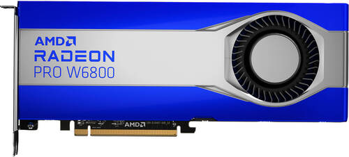
AMD Radeon PRO W6800
$2,249
|
8960 Shaders
24GB GDDR7
1337MHz
|
3840 Shaders
32GB GDDR6
2320MHz
|
|
Peak AI Performance
766.69 TFLOPS
FP4 Tensor Sparse
|
Peak AI Performance
35.64 TFLOPS
FP16
|
|
FP32
23.96 TFLOPS
|
FP32
17.82 TFLOPS
|
|
FP16
23.96 TFLOPS
|
FP16
35.64 TFLOPS
|
|
Form Factor
PCIe Card
1.0-Slots
|
Form Factor
PCIe Card
2.0-Slots
|
|
TDP
70W
|
TDP
250W
|
|
-
-
-
-
-
|
Power Connectors
1x 6-Pin
1x 8-Pin
-
-
|
|
GB6 OpenCL N/A
0%
|
|
|
GB6 Metal N/A
0%
|
|
|
GB6 Vulkan N/A
0%
|
|
GB5 OpenCL N/A
0%
|
GB5 OpenCL N/A
0%
|
|
GB5 CUDA N/A
0%
|
GB5 CUDA N/A
0%
|
|
GB5 Metal N/A
0%
|
GB5 Metal N/A
0%
|
|
GB5 Vulkan N/A
0%
|
GB5 Vulkan N/A
0%
|
|
OCT 2020.1 N/A
0%
|
OCT 2020.1 N/A
0%
|
|
OCT Metal N/A
0%
|
OCT Metal N/A
0%
|
|
Peak AI
Performance
766.69 TFLOPS
FP4 Tensor Sparse
|
Peak AI
Performance
35.64 TFLOPS
FP16
|
|
FP4
383.35 TFLOPS
Tensor
766.69 TFLOPS
Tensor Sparse
|
-
-
-
|
|
FP8
-
191.67 TFLOPS
Tensor (FP16 Accumulate)
383.34 TFLOPS
Tensor (FP16 Accumulate) Sparse
191.67 TFLOPS
Tensor (FP32 Accumulate)
383.34 TFLOPS
Tensor (FP32 Accumulate) Sparse
|
-
-
-
-
-
-
|
|
FP16
23.96 TFLOPS
95.84 TFLOPS
Tensor (FP16 Accumulate)
191.67 TFLOPS
Tensor (FP16 Accumulate) Sparse
95.84 TFLOPS
Tensor (FP32 Accumulate)
191.67 TFLOPS
Tensor (FP32 Accumulate) Sparse
|
FP16
35.64 TFLOPS
-
-
-
-
|
|
FP32
23.96 TFLOPS
-
-
|
FP32
17.82 TFLOPS
-
-
|
|
FP64
370 GFLOPS
-
|
FP64
1.11 TFLOPS
-
|
|
BF16
23.96 TFLOPS
95.84 TFLOPS
Tensor
191.67 TFLOPS
Tensor Sparse
|
-
-
-
-
|
|
TF32
47.92 TFLOPS
Tensor
95.84 TFLOPS
Tensor Sparse
|
-
-
-
|
|
-
-
-
|
-
-
-
|
|
INT8
-
191.67 TOPS
Tensor
383.34 TOPS
Tensor Sparse
|
-
-
-
-
|
|
INT32
11.98 TOPS
|
-
-
|
|
Ray Tracing
72.7 TOPS
|
-
-
|
|
Pixel
Fillrate
128.352 GPixel/s
|
Pixel
Fillrate
222.72 GPixel/s
|
|
-
-
|
-
-
|
|
Texture
Fillrate
374.36 GTexel/s
|
Texture
Fillrate
556.8 GTexel/s
|
|
Manufacturer
NVIDIA
|
Manufacturer
AMD
|
|
Chip Designer
NVIDIA
|
Chip Designer
AMD
|
|
Architecture
Blackwell
|
Architecture
RDNA 2
|
|
Family
RTX PRO Blackwell
|
Family
Radeon PRO W
|
|
Codename
NV193
GB203
-
-
|
Codename
Sienna Cichlid
Navi 21
Variant
Navi 21 XL GL
|
|
Market Segment
Workstation
|
Market Segment
Workstation
|
|
Release Date
8/11/2025
|
Release Date
6/8/2021
|
|
Foundry
TSMC
-
|
Foundry
TSMC
-
|
|
Fabrication Node
4NP
-
|
Fabrication Node
N7
-
|
|
Die Size
378 mm²
-
|
Die Size
520 mm²
-
|
|
Transistor Count
45.6 Billion
-
|
Transistor Count
26.8 Billion
-
|
|
Transistor Density
120.63M/mm²
-
|
Transistor Density
51.56M/mm²
-
|
|
Form
PCIe Card
|
Form
PCIe Card
|
|
Shading Units
8960 Shaders
-
|
Shading Units
3840 Shaders
-
|
|
Texture Mapping Units
280 TMUs
|
Texture Mapping Units
240 TMUs
|
|
Render Output Units
96 ROPs
|
Render Output Units
96 ROPs
|
|
Tensor Cores
280 T-Cores
|
-
-
|
|
Ray-Tracing Cores
70 RT-Cores
|
Ray-Tracing Cores
60 RT-Cores
|
|
Streaming Multiprocessors
70 SMs
|
-
-
|
|
-
-
|
Compute Units
60 CUs
|
|
-
-
|
-
-
|
|
-
-
|
-
-
|
|
-
-
790MHz Base
1337MHz
|
-
-
2075MHz Base
2320MHz
|
|
-
-
|
L0
32KB/WGP
|
|
L1
64KB/SM Tex
128KB/SM
-
-
|
L1
-
-
-
128KB/Array
|
|
L2
48MB Shared
|
L2
4MB Shared
|
|
-
-
-
|
L3
128MB Shared
1.66TB/s
|
|
24GB
GDDR7
ECC
|
32GB
GDDR6
-
|
|
Bus Width
192Bit
|
Bus Width
256Bit
|
|
Clock
1125MHz
Transfer Rate
18GT/s
Bandwidth
432GB/s
|
Clock
2000MHz
Transfer Rate
16GT/s
Bandwidth
512GB/s
|
|
-
-
-
-
-
-
-
-
-
|
-
-
-
-
-
-
-
-
-
|
|
TDP
70W
|
TDP
250W
|
|
-
-
|
-
-
|
|
-
-
-
-
-
-
-
-
-
-
-
-
-
-
-
-
-
-
-
-
-
-
-
-
-
-
4x DisplayPort 2.1
-
-
-
-
-
-
-
-
-
-
-
-
|
-
-
-
-
-
-
-
-
-
-
-
-
-
-
-
-
-
6x mini-DisplayPort 1.4
-
-
-
-
-
-
-
-
-
-
-
-
-
-
-
-
-
-
-
-
-
|
|
Max Resolution
7680x4320
|
Max Resolution
7680x4320
|
|
Max Resolution Refresh Rate
165Hz
|
Max Resolution Refresh Rate
120Hz
|
|
Variable Refresh Rate
G-Sync
FreeSync
-
|
Variable Refresh Rate
-
FreeSync
-
|
|
Display Stream Compression (DSC)
Supported
|
Display Stream Compression (DSC)
Supported
|
|
Multi Monitor Support
4
|
Multi Monitor Support
4
|
|
Content Protection
HDCP 2.3
|
Content Protection
HDCP 2.3
|
|
Model
2x NVENC 9
|
Model
VCN 3.0
|
|
Codec
-
-
-
-
-
-
-
-
AVC (H.264)
HEVC (H.265)
-
AV1
-
-
|
Codec
-
-
-
-
-
-
-
-
AVC (H.264)
HEVC (H.265)
-
-
-
-
|
|
Model
2x NVDEC 6
|
Model
VCN 3.0
|
|
Codec
MPEG-1
MPEG-2
MPEG-4
-
VC-1
VP8
VP9
-
AVC (H.264)
HEVC (H.265)
-
AV1
-
-
|
Codec
MPEG-1
MPEG-2
MPEG-4
JPEG
VC-1
-
VP9
-
AVC (H.264)
HEVC (H.265)
-
AV1
-
-
|
|
Direct X
12
Direct 3D
12_3
|
Direct X
12
Direct 3D
12_2
|
|
OpenGL
4.6
OpenCL
3.0
Vulkan
1.3
|
OpenGL
4.6
OpenCL
2.1
Vulkan
1.2
|
|
Shader Model
6.8
CUDA
12.8
-
-
PureVideo HD
VP13
VDPAU
Feature Set M
|
Shader Model
6.7
-
-
GFX
10.3
-
-
-
-
|
|
-
-
-
1x Fan
|
-
-
-
1x Fan
|
|
-
-
-
-
-
-
-
-
|
Power Connectors
-
-
1x 6-Pin
1x 8-Pin
-
-
-
|
|
Slots Required
1.0
PCIe Version
5.0
PCIe Lanes
16
|
Slots Required
2.0
PCIe Version
4.0
PCIe Lanes
16
|
|
Multi GPU Support
Supported
Type
NVLink
|
Multi GPU Support
Supported
Type
CrossFire XDMA
|
|
Height
69 mm (2.72 in)
Width
167 mm (6.57 in)
Depth
20 mm (0.79 in)
|
Height
111 mm (4.37 in)
Width
267 mm (10.51 in)
Depth
40 mm (1.57 in)
|


Copy Link