NVIDIA RTX PRO 4500 Blackwell vs Radeon Pro Vega II Duo
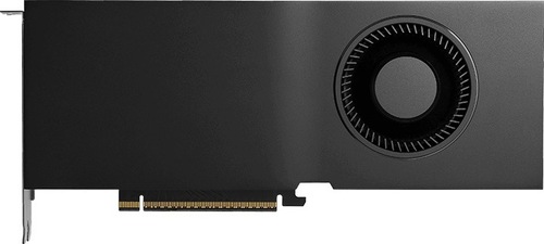
NVIDIA RTX PRO 4500 Blackwell
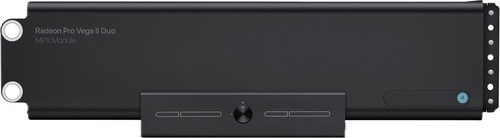
Radeon Pro Vega II Duo
$5,600
|
10496 Shaders
32GB GDDR7
2617MHz
|
2x 4096 Shaders
64GB (2x 32GB) HBM2
1720MHz
|
|
Peak AI Performance
1.76 PFLOPS
FP4 Tensor Sparse
|
Peak AI Performance
56.36 TFLOPS
FP16
|
|
FP32
54.94 TFLOPS
|
FP32
28.18 TFLOPS
|
|
FP16
54.94 TFLOPS
|
FP16
56.36 TFLOPS
|
|
Form Factor
PCIe Card
2.0-Slots
|
Form Factor
MPX
4.0-Slots
|
|
TDP
200W
|
TDP
475W
|
|
Power Connectors
-
-
-
1x 16-Pin 12VHPWR
|
-
-
-
-
-
|
|
GB6 OpenCL N/A
0%
|
|
|
GB6 Metal N/A
0%
|
|
|
GB6 Vulkan N/A
0%
|
GB6 Vulkan N/A
0%
|
|
GB5 OpenCL N/A
0%
|
GB5 OpenCL N/A
0%
|
|
GB5 CUDA N/A
0%
|
GB5 CUDA N/A
0%
|
|
GB5 Metal N/A
0%
|
GB5 Metal N/A
0%
|
|
GB5 Vulkan N/A
0%
|
GB5 Vulkan N/A
0%
|
|
OCT 2020.1 N/A
0%
|
OCT 2020.1 N/A
0%
|
|
OCT Metal N/A
0%
|
OCT Metal N/A
0%
|
|
Peak AI
Performance
1.76 PFLOPS
FP4 Tensor Sparse
|
Peak AI
Performance
56.36 TFLOPS
FP16
|
|
FP4
878.98 TFLOPS
Tensor
1.76 PFLOPS
Tensor Sparse
|
-
-
-
|
|
FP8
-
439.49 TFLOPS
Tensor (FP16 Accumulate)
878.98 TFLOPS
Tensor (FP16 Accumulate) Sparse
439.49 TFLOPS
Tensor (FP32 Accumulate)
878.98 TFLOPS
Tensor (FP32 Accumulate) Sparse
|
-
-
-
-
-
-
|
|
FP16
54.94 TFLOPS
219.74 TFLOPS
Tensor (FP16 Accumulate)
439.49 TFLOPS
Tensor (FP16 Accumulate) Sparse
219.74 TFLOPS
Tensor (FP32 Accumulate)
439.49 TFLOPS
Tensor (FP32 Accumulate) Sparse
|
FP16
56.36 TFLOPS
-
-
-
-
|
|
FP32
54.94 TFLOPS
-
-
|
FP32
28.18 TFLOPS
-
-
|
|
FP64
860 GFLOPS
-
|
FP64
7.05 TFLOPS
-
|
|
BF16
54.94 TFLOPS
219.74 TFLOPS
Tensor
439.49 TFLOPS
Tensor Sparse
|
-
-
-
-
|
|
TF32
109.87 TFLOPS
Tensor
219.74 TFLOPS
Tensor Sparse
|
-
-
-
|
|
-
-
-
|
-
-
-
|
|
INT8
-
439.49 TOPS
Tensor
878.98 TOPS
Tensor Sparse
|
-
-
-
-
|
|
INT32
27.47 TOPS
|
-
-
|
|
Ray Tracing
166.6 TOPS
|
-
-
|
|
Pixel
Fillrate
293.104 GPixel/s
|
Pixel
Fillrate
110.08 GPixel/s
|
|
-
-
|
-
-
|
|
Texture
Fillrate
858.376 GTexel/s
|
Texture
Fillrate
440.32 GTexel/s
|
|
Manufacturer
NVIDIA
|
Manufacturer
Apple
|
|
Chip Designer
NVIDIA
|
Chip Designer
AMD
|
|
Architecture
Blackwell
|
Architecture
GCN 5
|
|
Family
RTX PRO Blackwell
|
Family
Radeon Pro Vega
|
|
Codename
NV193
GB203
-
-
|
Codename
Moonshot
Vega 20
Variant
Vega 20 XTXA
|
|
Market Segment
Workstation
|
Market Segment
Workstation
|
|
Release Date
3/18/2025
|
Release Date
12/1/2019
|
|
Foundry
TSMC
-
|
Foundry
TSMC
-
|
|
Fabrication Node
4NP
-
|
Fabrication Node
N7
-
|
|
Die Size
378 mm²
-
|
Die Size
2x 331 mm²
-
|
|
Transistor Count
45.6 Billion
-
|
Transistor Count
2x 13.2 Billion
-
|
|
Transistor Density
120.63M/mm²
-
|
Transistor Density
39.97M/mm²
-
|
|
Form
PCIe Card
|
Form
MPX
|
|
Shading Units
10496 Shaders
-
|
Shading Units
2x 4096 Shaders
-
|
|
Texture Mapping Units
328 TMUs
|
Texture Mapping Units
2x 256 TMUs
|
|
Render Output Units
112 ROPs
|
Render Output Units
2x 64 ROPs
|
|
Tensor Cores
328 T-Cores
|
-
-
|
|
Ray-Tracing Cores
82 RT-Cores
|
-
-
|
|
Streaming Multiprocessors
82 SMs
|
-
-
|
|
-
-
|
Compute Units
2x 64 CUs
|
|
-
-
|
-
-
|
|
-
-
|
-
-
|
|
-
-
-
2617MHz
|
-
-
-
1720MHz
|
|
-
-
|
-
-
|
|
L1
64KB/SM Tex
128KB/SM
-
-
|
L1
-
-
16KB/CU
-
|
|
L2
64MB Shared
|
L2
4MB Shared
|
|
-
-
-
|
-
-
-
|
|
32GB
GDDR7
ECC
|
64GB (2x 32GB)
HBM2
-
|
|
Bus Width
256Bit
|
Bus Width
4096Bit
|
|
Clock
1750MHz
Transfer Rate
28GT/s
Bandwidth
896GB/s
|
Clock
1000MHz
Transfer Rate
2GT/s
Bandwidth
1024GB/s
|
|
-
-
-
-
-
-
-
-
-
|
-
-
-
-
-
-
-
-
-
|
|
TDP
200W
|
TDP
475W
|
|
-
-
|
-
-
|
|
-
-
-
-
-
-
-
-
-
-
-
-
-
-
-
-
-
-
-
-
-
-
-
-
-
-
4x DisplayPort 2.1
-
-
-
-
-
-
-
-
-
-
-
-
|
-
-
-
-
-
-
-
-
-
-
-
-
-
-
-
-
-
-
-
-
-
-
-
-
-
-
-
-
-
-
-
-
-
-
-
1x HDMI 2.0
-
-
4x Thunderbolt 3 (40Gbps)
|
|
Max Resolution
7680x4320
|
Max Resolution
7680x4320
|
|
Max Resolution Refresh Rate
165Hz
|
Max Resolution Refresh Rate
60Hz
|
|
Variable Refresh Rate
G-Sync
FreeSync
-
|
Variable Refresh Rate
-
FreeSync
-
|
|
Display Stream Compression (DSC)
Supported
|
Display Stream Compression (DSC)
Not Supported
|
|
Multi Monitor Support
4
|
Multi Monitor Support
3
|
|
Content Protection
HDCP 2.3
|
Content Protection
HDCP 2.2
|
|
Model
2x NVENC 9
|
Model
VCE 4.1
|
|
Codec
-
-
-
-
-
-
-
-
AVC (H.264)
HEVC (H.265)
-
AV1
-
-
|
Codec
-
-
-
-
-
-
-
-
AVC (H.264)
HEVC (H.265)
-
-
-
-
|
|
Model
2x NVDEC 6
|
Model
UVD 7.2
|
|
Codec
MPEG-1
MPEG-2
MPEG-4
-
VC-1
VP8
VP9
-
AVC (H.264)
HEVC (H.265)
-
AV1
-
-
|
Codec
MPEG-1
MPEG-2
MPEG-4
JPEG
VC-1
-
-
-
AVC (H.264)
HEVC (H.265)
-
-
-
-
|
|
Direct X
12
Direct 3D
12_3
|
Direct X
12
Direct 3D
12_1
|
|
OpenGL
4.6
OpenCL
3.0
Vulkan
1.3
|
OpenGL
4.6
OpenCL
2.1
Vulkan
1.3
|
|
Shader Model
6.8
CUDA
12.8
-
-
PureVideo HD
VP13
VDPAU
Feature Set M
|
Shader Model
6.7
-
-
GFX
9
-
-
-
-
|
|
-
-
-
1x Fan
|
-
-
-
-
|
|
Power Connectors
-
-
-
-
-
-
1x 16-Pin 12VHPWR
|
-
-
-
-
-
-
-
-
|
|
Slots Required
2.0
PCIe Version
5.0
PCIe Lanes
16
|
Slots Required
4.0
PCIe Version
3.0
PCIe Lanes
16
|
|
Multi GPU Support
Supported
Type
NVLink
|
Multi GPU Support
Supported
Type
CrossFire XDMA
|
|
Height
111.8 mm (4.4 in)
Width
266.7 mm (10.5 in)
Depth
40 mm (1.57 in)
|
-
-
-
-
-
-
|


Copy Link