NVIDIA RTX PRO 5000 Blackwell vs NVIDIA Quadro RTX 6000 Passive
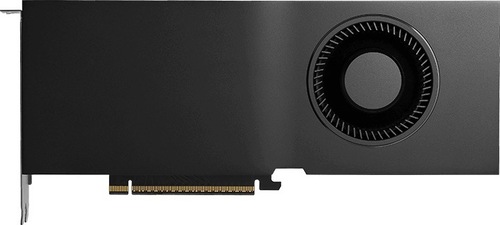
NVIDIA RTX PRO 5000 Blackwell

NVIDIA Quadro RTX 6000 Passive
$6,299
|
14080 Shaders
48GB GDDR7
2617MHz
|
4608 Shaders
24GB GDDR6
1560MHz
|
|
Peak AI Performance
2.36 PFLOPS
FP4 Tensor Sparse
|
Peak AI Performance
460.06 TOPS
INT4 Tensor
|
|
FP32
73.69 TFLOPS
|
FP32
14.38 TFLOPS
|
|
FP16
73.69 TFLOPS
|
FP16
28.75 TFLOPS
|
|
Form Factor
PCIe Card
2.0-Slots
|
Form Factor
PCIe Card
2.0-Slots
|
|
TDP
300W
|
TDP
260W
|
|
Power Connectors
-
-
-
1x 16-Pin 12VHPWR
|
Power Connectors
1x 6-Pin
1x 8-Pin
-
-
|
|
GB6 OpenCL N/A
0%
|
GB6 OpenCL N/A
0%
|
|
GB6 Metal N/A
0%
|
GB6 Metal N/A
0%
|
|
GB6 Vulkan N/A
0%
|
GB6 Vulkan N/A
0%
|
|
GB5 OpenCL N/A
0%
|
GB5 OpenCL N/A
0%
|
|
GB5 CUDA N/A
0%
|
GB5 CUDA N/A
0%
|
|
GB5 Metal N/A
0%
|
GB5 Metal N/A
0%
|
|
GB5 Vulkan N/A
0%
|
GB5 Vulkan N/A
0%
|
|
OCT 2020.1 N/A
0%
|
OCT 2020.1 N/A
0%
|
|
OCT Metal N/A
0%
|
OCT Metal N/A
0%
|
|
Peak AI
Performance
2.36 PFLOPS
FP4 Tensor Sparse
|
Peak AI
Performance
460.06 TOPS
INT4 Tensor
|
|
FP4
1.18 PFLOPS
Tensor
2.36 PFLOPS
Tensor Sparse
|
-
-
-
|
|
FP8
-
589.56 TFLOPS
Tensor (FP16 Accumulate)
1.18 PFLOPS
Tensor (FP16 Accumulate) Sparse
589.56 TFLOPS
Tensor (FP32 Accumulate)
1.18 PFLOPS
Tensor (FP32 Accumulate) Sparse
|
-
-
-
-
-
-
|
|
FP16
73.69 TFLOPS
294.78 TFLOPS
Tensor (FP16 Accumulate)
589.56 TFLOPS
Tensor (FP16 Accumulate) Sparse
294.78 TFLOPS
Tensor (FP32 Accumulate)
589.56 TFLOPS
Tensor (FP32 Accumulate) Sparse
|
FP16
28.75 TFLOPS
115.02 TFLOPS
Tensor (FP16 Accumulate)
-
115.02 TFLOPS
Tensor (FP32 Accumulate)
-
|
|
FP32
73.69 TFLOPS
-
-
|
FP32
14.38 TFLOPS
-
-
|
|
FP64
1.15 TFLOPS
-
|
FP64
450 GFLOPS
-
|
|
BF16
73.69 TFLOPS
294.78 TFLOPS
Tensor
589.56 TFLOPS
Tensor Sparse
|
-
-
-
-
|
|
TF32
147.39 TFLOPS
Tensor
294.78 TFLOPS
Tensor Sparse
|
-
-
-
|
|
-
-
-
|
INT4
460.06 TOPS
Tensor
-
|
|
INT8
-
589.56 TOPS
Tensor
1.18 POPS
Tensor Sparse
|
INT8
-
230.03 TOPS
Tensor
-
|
|
INT32
36.85 TOPS
|
-
-
|
|
Ray Tracing
223.5 TOPS
|
Ray Tracing
43.4 TOPS
|
|
Pixel
Fillrate
460.592 GPixel/s
|
Pixel
Fillrate
149.76 GPixel/s
|
|
-
-
|
-
-
|
|
Texture
Fillrate
1151.48 GTexel/s
|
Texture
Fillrate
449.28 GTexel/s
|
|
Manufacturer
NVIDIA
|
Manufacturer
NVIDIA
|
|
Chip Designer
NVIDIA
|
Chip Designer
NVIDIA
|
|
Architecture
Blackwell
|
Architecture
Turing
|
|
Family
RTX PRO Blackwell
|
Family
Quadro RTX
|
|
Codename
NV192
GB202
-
-
|
Codename
NV162
TU102
Variant
TU102-875-A1
|
|
Market Segment
Workstation
|
Market Segment
Workstation
|
|
Release Date
3/18/2025
|
Release Date
8/13/2018
|
|
Foundry
TSMC
-
|
Foundry
TSMC
-
|
|
Fabrication Node
4NP
-
|
Fabrication Node
12FFN
-
|
|
Die Size
762 mm²
-
|
Die Size
754 mm²
-
|
|
Transistor Count
92.2 Billion
-
|
Transistor Count
18.6 Billion
-
|
|
Transistor Density
121.07M/mm²
-
|
Transistor Density
24.67M/mm²
-
|
|
Form
PCIe Card
|
Form
PCIe Card
|
|
Shading Units
14080 Shaders
-
|
Shading Units
4608 Shaders
-
|
|
Texture Mapping Units
440 TMUs
|
Texture Mapping Units
288 TMUs
|
|
Render Output Units
176 ROPs
|
Render Output Units
96 ROPs
|
|
Tensor Cores
440 T-Cores
|
Tensor Cores
576 T-Cores
|
|
Ray-Tracing Cores
110 RT-Cores
|
Ray-Tracing Cores
72 RT-Cores
|
|
Streaming Multiprocessors
110 SMs
|
Streaming Multiprocessors
72 SMs
|
|
-
-
|
-
-
|
|
-
-
|
-
-
|
|
-
-
|
-
-
|
|
-
-
-
2617MHz
|
-
-
1305MHz Base
1560MHz
|
|
-
-
|
-
-
|
|
L1
64KB/SM Tex
128KB/SM
-
-
|
L1
32KB/SM Tex
64KB/SM
-
-
|
|
L2
96MB Shared
|
L2
6MB Shared
|
|
-
-
-
|
-
-
-
|
|
48GB
GDDR7
ECC
|
24GB
GDDR6
ECC
|
|
Bus Width
384Bit
|
Bus Width
384Bit
|
|
Clock
1750MHz
Transfer Rate
28GT/s
Bandwidth
1344GB/s
|
Clock
1750MHz
Transfer Rate
14GT/s
Bandwidth
672GB/s
|
|
-
-
-
-
-
-
-
-
-
|
-
-
-
-
-
-
-
-
-
|
|
TDP
300W
|
TDP
260W
|
|
-
-
|
-
-
|
|
-
-
-
-
-
-
-
-
-
-
-
-
-
-
-
-
-
-
-
-
-
-
-
-
-
-
4x DisplayPort 2.1
-
-
-
-
-
-
-
-
-
-
-
-
|
-
-
-
-
-
-
-
-
-
-
-
-
-
-
-
-
-
-
-
-
-
-
-
-
-
-
-
-
-
-
-
-
-
-
-
-
-
-
-
No Ports
|
|
Max Resolution
7680x4320
|
Max Resolution
7680x4320
|
|
Max Resolution Refresh Rate
165Hz
|
Max Resolution Refresh Rate
120Hz
|
|
Variable Refresh Rate
G-Sync
FreeSync
-
|
Variable Refresh Rate
G-Sync
FreeSync
-
|
|
Display Stream Compression (DSC)
Supported
|
Display Stream Compression (DSC)
Supported
|
|
Multi Monitor Support
4
|
Multi Monitor Support
4
|
|
Content Protection
HDCP 2.3
|
Content Protection
HDCP 2.2
|
|
Model
2x NVENC 9
|
Model
NVENC 7
|
|
Codec
-
-
-
-
-
-
-
-
AVC (H.264)
HEVC (H.265)
-
AV1
-
-
|
Codec
-
-
-
-
-
-
-
-
AVC (H.264)
HEVC (H.265)
-
-
-
-
|
|
Model
2x NVDEC 6
|
Model
NVDEC 4
|
|
Codec
MPEG-1
MPEG-2
MPEG-4
-
VC-1
VP8
VP9
-
AVC (H.264)
HEVC (H.265)
-
AV1
-
-
|
Codec
MPEG-1
MPEG-2
MPEG-4
-
VC-1
VP8
VP9
-
AVC (H.264)
HEVC (H.265)
-
-
-
-
|
|
Direct X
12
Direct 3D
12_3
|
Direct X
12
Direct 3D
12_2
|
|
OpenGL
4.6
OpenCL
3.0
Vulkan
1.3
|
OpenGL
4.6
OpenCL
3.0
Vulkan
1.2
|
|
Shader Model
6.8
CUDA
12.8
-
-
PureVideo HD
VP13
VDPAU
Feature Set M
|
Shader Model
6.6
CUDA
7.5
-
-
PureVideo HD
VP10
VDPAU
Feature Set J
|
|
-
-
-
1x Fan
|
-
-
-
-
|
|
Power Connectors
-
-
-
-
-
-
1x 16-Pin 12VHPWR
|
Power Connectors
-
-
1x 6-Pin
1x 8-Pin
-
-
-
|
|
Slots Required
2.0
PCIe Version
5.0
PCIe Lanes
16
|
Slots Required
2.0
PCIe Version
3.0
PCIe Lanes
16
|
|
Multi GPU Support
Supported
Type
NVLink
|
Multi GPU Support
Supported
Type
2-way NVLink
|
|
Height
111.8 mm (4.4 in)
Width
266.7 mm (10.5 in)
Depth
40 mm (1.57 in)
|
Height
111 mm (4.37 in)
Width
267 mm (10.51 in)
Depth
40 mm (1.57 in)
|


Copy Link