NVIDIA Tesla P10 vs AMD FirePro S7150 X2
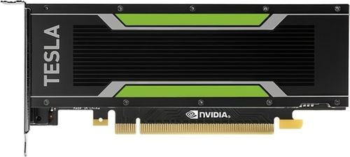
NVIDIA Tesla P10
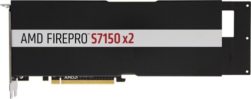
AMD FirePro S7150 X2
$3,999
|
3840 Shaders
24GB GDDR5
1493MHz
|
2x 1792 Shaders
32GB (2x 16GB) GDDR5
1050MHz
|
|
Peak AI Performance
45.87 TOPS
INT8
|
Peak AI Performance
7.53 TFLOPS
FP32
|
|
FP32
11.47 TFLOPS
|
FP32
7.53 TFLOPS
|
|
FP16
180 GFLOPS
|
-
-
|
|
Form Factor
PCIe Card
2.0-Slots
|
Form Factor
PCIe Card
2.0-Slots
|
|
TDP
250W
|
TDP
265W
|
|
Power Connectors
1x 6-Pin
1x 8-Pin
-
-
|
Power Connectors
1x 6-Pin
1x 8-Pin
-
-
|
|
GB6 OpenCL N/A
0%
|
GB6 OpenCL N/A
0%
|
|
GB6 Metal N/A
0%
|
GB6 Metal N/A
0%
|
|
GB6 Vulkan N/A
0%
|
GB6 Vulkan N/A
0%
|
|
GB5 OpenCL N/A
0%
|
GB5 OpenCL N/A
0%
|
|
GB5 CUDA N/A
0%
|
GB5 CUDA N/A
0%
|
|
GB5 Metal N/A
0%
|
GB5 Metal N/A
0%
|
|
GB5 Vulkan N/A
0%
|
GB5 Vulkan N/A
0%
|
|
OCT 2020.1 N/A
0%
|
OCT 2020.1 N/A
0%
|
|
OCT Metal N/A
0%
|
OCT Metal N/A
0%
|
|
Peak AI
Performance
45.87 TOPS
INT8
|
Peak AI
Performance
7.53 TFLOPS
FP32
|
|
-
-
-
|
-
-
-
|
|
-
-
-
-
-
-
|
-
-
-
-
-
-
|
|
FP16
180 GFLOPS
-
-
-
-
|
-
-
-
-
-
-
|
|
FP32
11.47 TFLOPS
-
-
|
FP32
7.53 TFLOPS
-
-
|
|
FP64
360 GFLOPS
-
|
FP64
470 GFLOPS
-
|
|
-
-
-
-
|
-
-
-
-
|
|
-
-
-
|
-
-
-
|
|
-
-
-
|
-
-
-
|
|
INT8
45.87 TOPS
-
-
|
-
-
-
-
|
|
-
-
|
-
-
|
|
-
-
|
-
-
|
|
Pixel
Fillrate
143.328 GPixel/s
|
Pixel
Fillrate
33.6 GPixel/s
|
|
-
-
|
-
-
|
|
Texture
Fillrate
358.32 GTexel/s
|
Texture
Fillrate
117.6 GTexel/s
|
|
Manufacturer
NVIDIA
|
Manufacturer
AMD
|
|
Chip Designer
NVIDIA
|
Chip Designer
AMD
|
|
Architecture
Pascal
|
Architecture
GCN 3
|
|
Family
Tesla P
|
Family
FirePro S
|
|
Codename
NV132
GP102
Variant
GP102-890-A1
|
Codename
Tonga
-
Variant
Tonga Pro GL
|
|
Market Segment
Server
|
Market Segment
Server
|
|
Release Date
9/13/2016
|
Release Date
2/1/2016
|
|
Foundry
TSMC
-
|
Foundry
TSMC
-
|
|
Fabrication Node
16FF
-
|
Fabrication Node
28nm
-
|
|
Die Size
471 mm²
-
|
Die Size
2x 359 mm²
-
|
|
Transistor Count
11.8 Billion
-
|
Transistor Count
2x 5 Billion
-
|
|
Transistor Density
25.05M/mm²
-
|
Transistor Density
13.93M/mm²
-
|
|
Form
PCIe Card
|
Form
PCIe Card
|
|
Shading Units
3840 Shaders
-
|
Shading Units
2x 1792 Shaders
-
|
|
Texture Mapping Units
240 TMUs
|
Texture Mapping Units
2x 112 TMUs
|
|
Render Output Units
96 ROPs
|
Render Output Units
2x 32 ROPs
|
|
-
-
|
-
-
|
|
-
-
|
-
-
|
|
Streaming Multiprocessors
30 SMs
|
-
-
|
|
-
-
|
Compute Units
2x 28 CUs
|
|
-
-
|
-
-
|
|
Graphics Processing Clusters
6 GPCs
|
-
-
|
|
-
-
1025MHz Base
1493MHz
|
-
-
-
1050MHz
|
|
-
-
|
-
-
|
|
L1
-
48KB/SM
-
-
|
L1
-
-
16KB/CU
-
|
|
L2
3MB Shared
|
L2
768KB Shared
|
|
-
-
-
|
-
-
-
|
|
24GB
GDDR5
-
|
32GB (2x 16GB)
GDDR5
-
|
|
Bus Width
384Bit
|
Bus Width
256Bit
|
|
Clock
1800MHz
Transfer Rate
7.2GT/s
Bandwidth
345.6GB/s
|
Clock
1250MHz
Transfer Rate
5GT/s
Bandwidth
160GB/s
|
|
-
-
-
-
-
-
-
-
-
|
-
-
-
-
-
-
-
-
-
|
|
TDP
250W
|
TDP
265W
|
|
-
-
|
-
-
|
|
-
-
-
-
-
-
-
-
-
-
-
-
-
-
-
-
-
-
-
-
-
-
-
-
-
-
-
-
-
-
-
-
-
-
-
-
-
-
-
No Ports
|
-
-
-
-
-
-
-
-
-
-
-
-
-
-
-
-
-
-
-
-
-
-
-
-
-
-
-
-
-
-
-
-
-
-
-
-
-
-
-
No Ports
|
|
Max Resolution
Unknown
|
Max Resolution
4096x2160
|
|
Max Resolution Refresh Rate
-
|
Max Resolution Refresh Rate
60Hz
|
|
Variable Refresh Rate
G-Sync
FreeSync
-
|
Variable Refresh Rate
-
FreeSync
-
|
|
Display Stream Compression (DSC)
Not Supported
|
Display Stream Compression (DSC)
Not Supported
|
|
Multi Monitor Support
Unknown
|
Multi Monitor Support
3
|
|
-
-
|
Content Protection
HDCP 1.4
|
|
Model
2x NVENC 4
|
Model
VCE 3.0
|
|
Codec
-
-
-
-
-
-
-
-
AVC (H.264)
HEVC (H.265)
-
-
-
-
|
Codec
-
-
-
-
-
-
-
-
AVC (H.264)
HEVC (H.265)
-
-
-
-
|
|
Model
NVDEC 3
|
Model
UVD 5.0
|
|
Codec
MPEG-1
MPEG-2
MPEG-4
-
VC-1
-
VP9
-
AVC (H.264)
HEVC (H.265)
-
-
-
-
|
Codec
MPEG-1
MPEG-2
MPEG-4
-
VC-1
-
-
-
AVC (H.264)
-
-
-
-
-
|
|
Direct X
12
Direct 3D
12_1
|
Direct X
12
Direct 3D
12_0
|
|
OpenGL
4.6
OpenCL
3.0
Vulkan
1.3
|
OpenGL
4.6
OpenCL
2.1
Vulkan
1.2
|
|
Shader Model
6.7
CUDA
6.1
-
-
PureVideo HD
VP8
VDPAU
Feature Set H
|
Shader Model
6.5
-
-
GFX
8
-
-
-
-
|
|
-
-
-
-
|
-
-
-
-
|
|
Power Connectors
-
-
1x 6-Pin
1x 8-Pin
-
-
-
|
Power Connectors
-
-
1x 6-Pin
1x 8-Pin
-
-
-
|
|
Slots Required
2.0
PCIe Version
3.0
PCIe Lanes
16
|
Slots Required
2.0
PCIe Version
3.0
PCIe Lanes
16
|
|
Multi GPU Support
Supported
-
-
|
Multi GPU Support
Supported
Type
CrossFire XDMA
|
|
Height
111 mm (4.37 in)
Width
267 mm (10.51 in)
Depth
40 mm (1.57 in)
|
Height
111 mm (4.37 in)
Width
241 mm (9.49 in)
Depth
37 mm (1.46 in)
|


Copy Link