NVIDIA V100 vs AMD FirePro S9300 X2
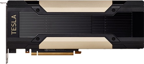
NVIDIA V100
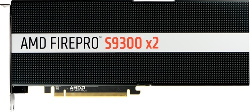
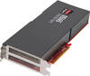
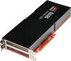
AMD FirePro S9300 X2
$5,999
|
5120 Shaders
32GB HBM2
1380MHz
|
2x 4096 Shaders
8GB (2x 4GB) HBM
850MHz
|
|
Peak AI Performance
113.05 TFLOPS
FP16 Tensor (FP16 Accumulate)
|
Peak AI Performance
13.93 TFLOPS
FP32
|
|
FP32
14.13 TFLOPS
|
FP32
13.93 TFLOPS
|
|
FP16
28.26 TFLOPS
|
-
-
|
|
Form Factor
PCIe Card
2.0-Slots
|
Form Factor
PCIe Card
2.0-Slots
|
|
TDP
250W
|
TDP
300W
|
|
Power Connectors
-
2x 8-Pin
-
-
|
Power Connectors
-
2x 8-Pin
-
-
|
|
GB6 OpenCL N/A
0%
|
|
|
GB6 Metal N/A
0%
|
GB6 Metal N/A
0%
|
|
GB6 Vulkan N/A
0%
|
GB6 Vulkan N/A
0%
|
|
GB5 OpenCL N/A
0%
|
GB5 OpenCL N/A
0%
|
|
GB5 CUDA N/A
0%
|
GB5 CUDA N/A
0%
|
|
GB5 Metal N/A
0%
|
GB5 Metal N/A
0%
|
|
GB5 Vulkan N/A
0%
|
GB5 Vulkan N/A
0%
|
|
OCT 2020.1 N/A
0%
|
OCT 2020.1 N/A
0%
|
|
OCT Metal N/A
0%
|
OCT Metal N/A
0%
|
|
Peak AI
Performance
113.05 TFLOPS
FP16 Tensor (FP16 Accumulate)
|
Peak AI
Performance
13.93 TFLOPS
FP32
|
|
-
-
-
|
-
-
-
|
|
-
-
-
-
-
-
|
-
-
-
-
-
-
|
|
FP16
28.26 TFLOPS
113.05 TFLOPS
Tensor (FP16 Accumulate)
-
-
-
|
-
-
-
-
-
-
|
|
FP32
14.13 TFLOPS
-
-
|
FP32
13.93 TFLOPS
-
-
|
|
FP64
7.07 TFLOPS
-
|
FP64
870 GFLOPS
-
|
|
-
-
-
-
|
-
-
-
-
|
|
-
-
-
|
-
-
-
|
|
-
-
-
|
-
-
-
|
|
INT8
56.53 TOPS
-
-
|
-
-
-
-
|
|
INT32
14.13 TOPS
|
-
-
|
|
-
-
|
-
-
|
|
Pixel
Fillrate
176.64 GPixel/s
|
Pixel
Fillrate
54.4 GPixel/s
|
|
-
-
|
-
-
|
|
Texture
Fillrate
441.6 GTexel/s
|
Texture
Fillrate
217.6 GTexel/s
|
|
Foundry
TSMC
-
|
Foundry
TSMC
-
|
|
Fabrication Node
12FFN
-
|
Fabrication Node
28nm
-
|
|
Die Size
815 mm²
-
|
Die Size
2x 596 mm²
-
|
|
Transistor Count
21.1 Billion
-
|
Transistor Count
2x 8.9 Billion
-
|
|
Transistor Density
25.89M/mm²
-
|
Transistor Density
14.93M/mm²
-
|
|
Form
PCIe Card
|
Form
PCIe Card
|
|
Shading Units
5120 Shaders
-
|
Shading Units
2x 4096 Shaders
-
|
|
Texture Mapping Units
320 TMUs
|
Texture Mapping Units
2x 256 TMUs
|
|
Render Output Units
128 ROPs
|
Render Output Units
2x 64 ROPs
|
|
Tensor Cores
640 T-Cores
|
-
-
|
|
-
-
|
-
-
|
|
Streaming Multiprocessors
80 SMs
|
-
-
|
|
-
-
|
Compute Units
2x 64 CUs
|
|
-
-
|
-
-
|
|
Graphics Processing Clusters
6 GPCs
|
-
-
|
|
-
-
1230MHz Base
1380MHz
|
-
-
-
850MHz
|
|
-
-
|
-
-
|
|
L1
-
128KB/SM
-
-
|
L1
-
-
16KB/CU
-
|
|
L2
6MB Shared
|
L2
2MB Shared
|
|
-
-
-
|
-
-
-
|
|
32GB
HBM2
-
|
8GB (2x 4GB)
HBM
-
|
|
Bus Width
4096Bit
|
Bus Width
4096Bit
|
|
Clock
875MHz
Transfer Rate
1.8GT/s
Bandwidth
896GB/s
|
Clock
500MHz
Transfer Rate
1GT/s
Bandwidth
512GB/s
|
|
-
-
-
-
-
-
-
-
-
|
-
-
-
-
-
-
-
-
-
|
|
TDP
250W
|
TDP
300W
|
|
-
-
|
-
-
|
|
-
-
-
-
-
-
-
-
-
-
-
-
-
-
-
-
-
-
-
-
-
-
-
-
-
-
-
-
-
-
-
-
-
-
-
-
-
-
-
No Ports
|
-
-
-
-
-
-
-
-
-
-
-
-
-
-
-
-
-
-
-
-
-
-
-
-
-
-
-
-
-
-
-
-
-
-
-
-
-
-
-
No Ports
|
|
Max Resolution
Unknown
|
Max Resolution
4096x2160
|
|
Max Resolution Refresh Rate
-
|
Max Resolution Refresh Rate
60Hz
|
|
Variable Refresh Rate
G-Sync
FreeSync
-
|
Variable Refresh Rate
-
FreeSync
-
|
|
Display Stream Compression (DSC)
Not Supported
|
Display Stream Compression (DSC)
Not Supported
|
|
Multi Monitor Support
Unknown
|
Multi Monitor Support
4
|
|
-
-
|
Content Protection
HDCP 1.4
|
|
Model
3x NVENC 5
|
Model
VCE 3.0
|
|
Codec
-
-
-
-
-
-
-
-
AVC (H.264)
HEVC (H.265)
-
-
-
-
|
Codec
-
-
-
-
-
-
-
-
AVC (H.264)
HEVC (H.265)
-
-
-
-
|
|
Model
NVDEC 3
|
Model
UVD 6.0
|
|
Codec
MPEG-1
MPEG-2
MPEG-4
-
VC-1
-
VP9
-
AVC (H.264)
HEVC (H.265)
-
-
-
-
|
Codec
MPEG-1
MPEG-2
MPEG-4
JPEG
VC-1
-
-
-
AVC (H.264)
HEVC (H.265)
-
-
-
-
|
|
Direct X
12
Direct 3D
12_1
|
Direct X
12
Direct 3D
12_0
|
|
OpenGL
4.6
OpenCL
3.0
-
-
|
OpenGL
4.6
OpenCL
2.1
Vulkan
1.2
|
|
Shader Model
6.7
CUDA
7.0
-
-
PureVideo HD
VP9
VDPAU
Feature Set I
|
Shader Model
6.5
-
-
GFX
8
-
-
-
-
|
|
-
-
-
-
|
-
-
-
-
|
|
Power Connectors
-
-
-
2x 8-Pin
-
-
-
|
Power Connectors
-
-
-
2x 8-Pin
-
-
-
|
|
Slots Required
2.0
PCIe Version
3.0
PCIe Lanes
16
|
Slots Required
2.0
PCIe Version
3.0
PCIe Lanes
16
|
|
Multi GPU Support
Supported
Type
NVLink
|
Multi GPU Support
Supported
Type
CrossFire XDMA
|
|
Height
111 mm (4.37 in)
Width
267 mm (10.51 in)
Depth
40 mm (1.57 in)
|
Height
111 mm (4.37 in)
Width
267 mm (10.51 in)
Depth
37 mm (1.46 in)
|


Copy Link