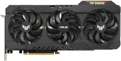
GeForce RTX 3080 Ti TUF OC
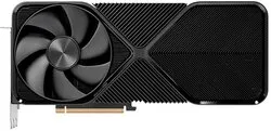
GeForce RTX 4080 Super
ASUS GeForce RTX 3080 Ti TUF OC vs NVIDIA GeForce RTX 4080 Super Full Specs
10,240 Shaders 1.78GHz | 10,240 Shaders 2.55GHz |
12GB GDDR6X912.4GB/s | 16GB GDDR6X716.8GB/s |
·· 36.56 TFLOPS | ·· 52.22 TFLOPS |
Form Factor PCIe Card | Form Factor PCIe Card |
TDP 350W | TDP 320W |
Power Connectors - 2x 8-Pin | Power Connectors 1x 16-Pin 12VHPWR - |
 GeForce RTX 3080 Ti TUF OC1.17 POPSINT4 Tensor Sparse
 GeForce RTX 4080 Super1.67 POPSINT4 Tensor Sparse
Clock Speed ··· | Clock Speed ··· |
Peak OPS 1.17 POPSINT4 Tensor Sparse | Peak OPS 1.67 POPSINT4 Tensor Sparse |
- | Tensor FP8-16 417.8 TFLOPSFP8-16 Tensor Sparse 835.6 TFLOPSTensor FP8-32 208.9 TFLOPSFP8-32 Tensor Sparse 417.8 TFLOPS |
Tensor FP16-16 146.2 TFLOPSFP16-16 Tensor Sparse 292.5 TFLOPSTensor FP16-32 73.11 TFLOPSFP16-32 Tensor Sparse 146.2 TFLOPS | Tensor FP16-16 208.9 TFLOPSFP16-16 Tensor Sparse 417.8 TFLOPSTensor FP16-32 104.4 TFLOPSFP16-32 Tensor Sparse 208.9 TFLOPS |
BF16 36.56 TFLOPSTensor BF16 73.11 TFLOPSBF16 Tensor Sparse 146.2 TFLOPS | BF16 52.22 TFLOPSTensor BF16 104.4 TFLOPSBF16 Tensor Sparse 208.9 TFLOPS |
Tensor TF32 36.56 TFLOPS | Tensor TF32 52.22 TFLOPS |
FP32 36.56 TFLOPS | FP32 52.22 TFLOPS |
FP64 571.2 GFLOPS | FP64 816 GFLOPS |
Tensor INT4 584.9 TOPS | Tensor INT4 835.6 TOPS |
Tensor INT8 292.5 TOPS | Tensor INT8 417.8 TOPS |
Ray 55.14 TOPS | Ray 120.7 TOPS |
Pixel Rate 199.9 GPixel/s | Pixel Rate 285.6 GPixel/s |
Texture Rate 571.2 GTexel/s | Texture Rate 816 GTexel/s |
Shaders 10,240 Shaders | Shaders 10,240 Shaders |
TMUs 320 TMUs | TMUs 320 TMUs |
ROPs 112 ROPs | ROPs 112 ROPs |
Tensor Cores 320 T-Cores | Tensor Cores 320 T-Cores |
RT Cores 80 RT-Cores | RT Cores 80 RT-Cores |
SMs 80 SMs | SMs 80 SMs |
Base Clock 1.4GHz | Base Clock 2.29GHz |
Boost Clock 1.78GHz | Boost Clock 2.55GHz |
L1 64KB/SM Tex | L1 64KB/SM Tex |
L2 Cache 6MB shared | L2 Cache 64MB shared |
12GB GDDR6X | 16GB GDDR6X |
Memory Bus 384-bit | Memory Bus 256-bit |
Memory Speed 19GT/s | Memory Speed 22.4GT/s |
Memory Bandwidth 912.4GB/s | Memory Bandwidth 716.8GB/s |
ECC No | ECC No |
TDP 350W | TDP 320W |
Max Temp 93°C Max | Max Temp 90°C Max |
Max Resolution 7680x4320 | Max Resolution 7680x4320 |
Refresh Rate Calculator 7680x4320 Resolution8K UHD Refresh Rate 60Hz | Refresh Rate Calculator 7680x4320 Resolution8K UHD Refresh Rate 60Hz |
Multi-Monitor 4 | Multi-Monitor 4 |
Adaptive Sync G-Sync FreeSync | Adaptive Sync G-Sync FreeSync |
DSC Supported | DSC Supported |
HDCP HDCP 2.3 | HDCP HDCP 2.3 |
3x DisplayPort 1.4 2x HDMI 2.1 | 3x DisplayPort 1.4 1x HDMI 2.1 |
Shader Model 6.6 | Shader Model 6.6 |
DirectX DirectX 12Direct3D 12_2 | DirectX DirectX 12Direct3D 12_3 |
OpenGL 4.6OpenCL 3Vulkan 1.2 | OpenGL 4.6OpenCL 3Vulkan 1.3 |
CUDA 8.6PureVideo HD VP11VDPAU Feature Set K | CUDA 8.9PureVideo HD VP12VDPAU Feature Set L |
Encoder NVENC 7 | Encoder 2x NVENC 8 |
Codec AVC (H.264) HEVC (H.265) - | Codec AVC (H.264) HEVC (H.265) AV1 |
Decoder NVDEC 5 | Decoder NVDEC 5 |
Codec MPEG-1 MPEG-2 MPEG-4 VC-1 VP8 VP9 AVC (H.264) HEVC (H.265) AV1 | Codec MPEG-1 MPEG-2 MPEG-4 VC-1 VP8 VP9 AVC (H.264) HEVC (H.265) AV1 |
Form Factor PCIe Card | Form Factor PCIe Card |
PCIe PCIe 4.0 x16 2.5-Slots | PCIe PCIe 4.0 x16 3-Slots |
Height 126.9mm (5")Width 299.9mm (11.81")Depth 51.7mm (2.04") | Height 137mm (5.39")Width 304mm (11.97")Depth 61mm (2.4") |
Cooling Open-Air 3x Fans | Cooling Open-Air 2x Fans |
Power Connectors 2x 8-Pin | Power Connectors 1x 16-Pin 12VHPWR |
Manufacturer | Manufacturer |
Chip Designer | Chip Designer |
Architecture | Architecture |
Family | Family |
Branding  | Branding  |
Codename NV172 | Codename NV183 |
Chip Variant GA102-200-KD-A1 | Chip Variant AD103-275-A1 |
Market Segment Desktop | Market Segment Desktop |
Release Date Jun 3, 2021 | Release Date Jan 8, 2024 |
Foundry Samsung | Foundry TSMC |
Fabrication Node 8N | Fabrication Node 4N |
Die Size 628mm² | Die Size 379mm² |
Transistor Count 28.3B | Transistor Count 45.9B |
Transistor Density 45.04 MTr/mm² | Transistor Density 121.2 MTr/mm² |
Desktops - | Desktops |