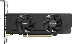
GeForce RTX 3050 OC Low Profile 6G

GeForce GTX 1660 Super
GIGABYTE GeForce RTX 3050 OC Low Profile 6G vs NVIDIA GeForce GTX 1660 Super Full Specs
2,304 Shaders 1.48GHz | 1,408 Shaders 1.78GHz |
6GB GDDR6168GB/s | 6GB GDDR6336GB/s |
·· 6.81 TFLOPS | ·· 5.03 TFLOPS |
Form Factor PCIe Card | Form Factor PCIe Card |
TDP 70W | TDP 125W |
Power Connectors - | Power Connectors 1x 8-Pin |
 GeForce RTX 3050 OC Low Profile 6G217.8 TOPSINT4 Tensor Sparse
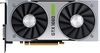 GeForce GTX 1660 Super10.05 TFLOPSFP16
Clock Speed ··· | Clock Speed ··· |
Peak OPS 217.8 TOPSINT4 Tensor Sparse | Peak OPS 10.05 TFLOPSFP16 |
Tensor FP16-16 27.22 TFLOPSFP16-16 Tensor Sparse 54.45 TFLOPSTensor FP16-32 13.61 TFLOPSFP16-32 Tensor Sparse 27.22 TFLOPS | - |
BF16 6.81 TFLOPSTensor BF16 13.61 TFLOPSBF16 Tensor Sparse 27.22 TFLOPS | - |
Tensor TF32 6.81 TFLOPS | Tensor TF32 - |
FP32 6.81 TFLOPS | FP32 5.03 TFLOPS |
FP64 106.3 GFLOPS | FP64 157.1 GFLOPS |
Tensor INT4 108.9 TOPS | Tensor INT4 - |
Tensor INT8 54.45 TOPS | - |
Ray 10.26 TOPS | Ray - |
Pixel Rate 47.3 GPixel/s | Pixel Rate 85.7 GPixel/s |
Texture Rate 106.3 GTexel/s | Texture Rate 157.1 GTexel/s |
Shaders 2,304 Shaders | Shaders 1,408 Shaders |
TMUs 72 TMUs | TMUs 88 TMUs |
ROPs 32 ROPs | ROPs 48 ROPs |
Tensor Cores 72 T-Cores | Tensor Cores - |
RT Cores 18 RT-Cores | RT Cores - |
SMs 18 SMs | SMs 22 SMs |
Base Clock 1.04GHz | Base Clock 1.53GHz |
Boost Clock 1.48GHz | Boost Clock 1.78GHz |
L1 64KB/SM Tex | L1 32KB/SM Tex |
L2 Cache 2MB shared | L2 Cache 1.5MB shared |
6GB GDDR6 | 6GB GDDR6 |
Memory Bus 96-bit | Memory Bus 192-bit |
Memory Speed 14GT/s | Memory Speed 14GT/s |
Memory Bandwidth 168GB/s | Memory Bandwidth 336GB/s |
ECC No | ECC No |
TDP 70W | TDP 125W |
Max Temp - | Max Temp 95°C Max |
Max Resolution 7680x4320 | Max Resolution 7680x4320 |
Refresh Rate Calculator 7680x4320 Resolution8K UHD Refresh Rate 60Hz | Refresh Rate Calculator 7680x4320 Resolution8K UHD Refresh Rate 60Hz |
Multi-Monitor 3 | Multi-Monitor 3 |
Adaptive Sync G-Sync FreeSync | Adaptive Sync G-Sync FreeSync |
DSC Supported | DSC Supported |
HDCP HDCP 2.3 | HDCP HDCP 2.2 |
2x DisplayPort 1.4 2x HDMI 2.1 - | 1x DisplayPort 1.4 1x HDMI 2.0 1x DVI-D Dual-Link |
Shader Model 6.6 | Shader Model 6.6 |
DirectX DirectX 12Direct3D 12_2 | DirectX DirectX 12Direct3D 12_1 |
OpenGL 4.6OpenCL 3Vulkan 1.2 | OpenGL 4.6OpenCL 3Vulkan 1.2 |
CUDA 8.6PureVideo HD VP11VDPAU Feature Set K | CUDA 7.5PureVideo HD VP10VDPAU Feature Set J |
Encoder NVENC 7 | Encoder NVENC 7 |
Codec AVC (H.264) HEVC (H.265) | Codec AVC (H.264) HEVC (H.265) |
Decoder NVDEC 5 | Decoder NVDEC 4 |
Codec MPEG-1 MPEG-2 MPEG-4 VC-1 VP8 VP9 AVC (H.264) HEVC (H.265) AV1 | Codec MPEG-1 MPEG-2 MPEG-4 VC-1 VP8 VP9 AVC (H.264) HEVC (H.265) - |
Form Factor PCIe Card | Form Factor PCIe Card |
PCIe PCIe 4.0 x8 1.8-Slots | PCIe PCIe 3.0 x16 - |
Height 69mm (2.72")Width 181mm (7.13")Depth 36mm (1.42") | - |
Cooling Open-Air 2x Fans | Cooling Open-Air 1x Fan |
Power Connectors - | Power Connectors 1x 8-Pin |
Manufacturer | Manufacturer |
Chip Designer | Chip Designer |
Architecture | Architecture |
Family | Family |
Branding  | Branding  |
Codename NV177 | Codename NV168 |
Chip Variant GA107-140-A1 | Chip Variant TU116-250-KA-A1 |
Market Segment Desktop | Market Segment Desktop |
Release Date Feb 2, 2024 | Release Date Oct 29, 2019 |
Foundry Samsung | Foundry TSMC |
Fabrication Node 8N | Fabrication Node 12FFN |
Die Size 200mm² | Die Size 284mm² |
Transistor Count 8.7B | Transistor Count 6.6B |
Transistor Density 43.5 MTr/mm² | Transistor Density 23.24 MTr/mm² |
Desktops - | Desktops |