A30
NVIDIA A30 Full Specs
3,584 Shaders 1.44GHz |
24GB HBM2933.1GB/s |
·· 10.32 TFLOPS |
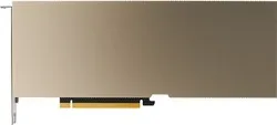
Form Factor PCIe Card |
TDP 165W |
 A301.32 POPSINT4 Tensor Sparse
3.35 PFLOPS FP4 Tensor SparseGeForce RTX 5090
x2.54Clock Speed ··· |
Peak OPS 1.32 POPSINT4 Tensor Sparse |
Tensor FP16-16 165.2 TFLOPSFP16-16 Tensor Sparse 330.3 TFLOPSTensor FP16-32 165.2 TFLOPSFP16-32 Tensor Sparse 330.3 TFLOPS |
BF16 20.64 TFLOPSTensor BF16 165.2 TFLOPSBF16 Tensor Sparse 330.3 TFLOPS |
Tensor TF32 82.58 TFLOPS |
FP32 10.32 TFLOPS |
FP64 5.16 TFLOPSTensor FP64 10.32 TFLOPS |
Tensor INT4 660.6 TOPS |
Tensor INT8 330.3 TOPS |
Pixel Rate 138.2 GPixel/s |
Texture Rate 322.6 GTexel/s |
Shaders 3,584 Shaders |
TMUs 224 TMUs |
ROPs 96 ROPs |
Tensor Cores 224 T-Cores |
SMs 56 SMs |
Base Clock 930MHz |
Boost Clock 1.44GHz |
L1 64KB/SM Tex |
L2 Cache 24MB shared |
24GB HBM2 |
Memory Bus 3072-bit |
Memory Speed 2.4GT/s |
Memory Bandwidth 933.1GB/s |
ECC No |
TDP 165W |
Adaptive Sync G-Sync FreeSync |
DSC Not Supported |
OpenCL 3Vulkan 1.2 |
CUDA 8PureVideo HD VP10VDPAU Feature Set J |
Decoder 5x NVDEC 4 |
Codec MPEG-1 MPEG-2 MPEG-4 VC-1 VP8 VP9 AVC (H.264) HEVC (H.265) |
Form Factor PCIe Card |
PCIe PCIe 4.0 x16 2-Slots |
Height 111mm (4.37")Width 267mm (10.51")Depth 40mm (1.57") |
Cooling Passive |
Multi-GPU Multi-GPU Support SupportedMulti-GPU Type NVLink |
Foundry TSMC |
Fabrication Node 7N |
Die Size 826mm² |
Transistor Count 54.2B |
Transistor Density 65.62 MTr/mm² |