GeForce G 100
NVIDIA GeForce G 100 Full Specs
8 Shaders 567MHz |
512MB DDR28GB/s |
·· 22.4 GFLOPS |
Form Factor PCIe Card |
TDP 35W |
 GeForce G 10022.4 GFLOPSFP32
3.35 PFLOPS FP4 Tensor SparseGeForce RTX 5090
x149646.63Clock Speed ·· |
Peak OPS 22.4 GFLOPSFP32 |
FP32 22.4 GFLOPS |
Pixel Rate 5.6 GPixel/s |
Texture Rate 11.2 GTexel/s |
Shaders 8 Shaders |
TMUs 8 TMUs |
ROPs 4 ROPs |
SM 1 SM |
Boost Clock 567MHz |
Shader Clock 1.4GHz |
L1 16KB/SM Tex |
L2 Cache 16KB shared |
512MB DDR2 |
Memory Bus 64-bit |
Memory Speed 1GT/s |
Memory Bandwidth 8GB/s |
ECC No |
TDP 35W |
Max Resolution 2560x1600 |
Refresh Rate Calculator 2560x1440 Resolution1440p QHD Refresh Rate 66Hz |
Multi-Monitor 2 |
DSC Not Supported |
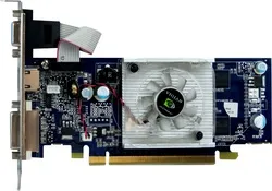
1x DVI-I Dual-Link 1x S-Video |
Shader Model 4 |
DirectX DirectX 11Direct3D 10_0 |
OpenGL 3.3OpenCL 1.1 |
CUDA 1.1PureVideo HD VP3VDPAU Feature Set B |
Decoder VP3 |
Form Factor PCIe Card |
PCIe PCIe 2.0 x16 1-Slots |
Height 69mm (2.72")Width 168mm (6.61")Depth 20mm (0.79") |
Cooling Open-Air 1x Fan |
Multi-GPU Multi-GPU Support SupportedMulti-GPU Type 2-way SLI |
Manufacturer |
Chip Designer |
Architecture |
Family |
Branding  |
Codename NV98 |
Chip Variant G98-409-U2 |
Market Segment Desktop |
Release Date Mar 10, 2009 |
Foundry TSMC |
Fabrication Node 65nm |
Die Size 86mm² |
Transistor Count 210M |
Transistor Density 2.44 MTr/mm² |