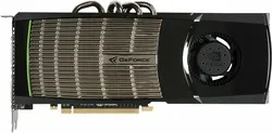
GeForce GTX 480
NVIDIA GeForce GTX 480 Full Specs
480 Shaders 701MHz |
1.5GB GDDR5177.4GB/s |
·· 1.34 TFLOPS |
Form Factor PCIe Card |
TDP 250W |
Power Connectors 1x 8-Pin 1x 6-Pin |
 GeForce GTX 4801.34 TFLOPSFP32
3.35 PFLOPS FP4 Tensor SparseGeForce RTX 5090
x2492.33Clock Speed ·· |
Peak OPS 1.34 TFLOPSFP32 |
FP32 1.34 TFLOPS |
FP64 168.1 GFLOPS |
Pixel Rate 67.3 GPixel/s |
Texture Rate 84.1 GTexel/s |
Shaders 480 Shaders |
TMUs 60 TMUs |
ROPs 48 ROPs |
SMs 15 SMs |
Boost Clock 701MHz |
Shader Clock 1.4GHz |
L1 64KB/SM |
L2 Cache 768KB shared |
1.5GB GDDR5 |
Memory Bus 384-bit |
Memory Speed 3.7GT/s |
Memory Bandwidth 177.4GB/s |
ECC No |
TDP 250W |
Max Resolution 2560x1600 |
Refresh Rate Calculator 2560x1440 Resolution1440p QHD Refresh Rate 66Hz |
Multi-Monitor 2 |
DSC Not Supported |
1x Mini HDMI 1.3 2x DVI-I Dual-Link |
Shader Model 5.1 |
DirectX DirectX 12Direct3D 11_0 |
OpenGL 4.6OpenCL 1.1 |
CUDA 2PureVideo HD VP4VDPAU Feature Set C |
Decoder VP4 |
Form Factor PCIe Card |
PCIe PCIe 2.0 x16 2-Slots |
Height 130mm (5.12")Width 267mm (10.51")Depth 38mm (1.5") |
Cooling Blower 1x Fan |
Power Connectors 1x 8-Pin, 1x 6-Pin |
Multi-GPU Multi-GPU Support SupportedMulti-GPU Type 4-way SLI |
Manufacturer |
Chip Designer |
Architecture |
Family |
Branding  |
Codename NVC0 |
Chip Variant GF100-030-A3 |
Market Segment Desktop |
Release Date Mar 26, 2010 |
Foundry TSMC |
Fabrication Node 40nm |
Die Size 529mm² |
Transistor Count 3B |
Transistor Density 5.67 MTr/mm² |