H100
NVIDIA H100 Full Specs
14,592 Shaders 1.75GHz |
80GB HBM2e2.04TB/s |
·· 51.22 TFLOPS |
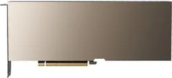
Form Factor PCIe Card |
TDP 350W |
Power Connectors 1x 16-Pin 12VHPWR |
 H1003.03 POPSINT8 Tensor Sparse
3.35 PFLOPS FP4 Tensor SparseGeForce RTX 5090
x1.11Clock Speed ··· |
Peak OPS 3.03 POPSINT8 Tensor Sparse |
Tensor FP8-16 1.51 PFLOPSFP8-16 Tensor Sparse 3.03 PFLOPSTensor FP8-32 1.51 PFLOPSFP8-32 Tensor Sparse 3.03 PFLOPS |
Tensor FP16-16 756.4 TFLOPSFP16-16 Tensor Sparse 1.51 PFLOPSTensor FP16-32 756.4 TFLOPSFP16-32 Tensor Sparse 1.51 PFLOPS |
BF16 102.4 TFLOPSTensor BF16 756.4 TFLOPSBF16 Tensor Sparse 1.51 PFLOPS |
Tensor TF32 378.2 TFLOPS |
FP32 51.22 TFLOPS |
FP64 25.61 TFLOPSTensor FP64 47.28 TFLOPS |
Tensor INT8 1.51 POPS |
Pixel Rate 42.1 GPixel/s |
Texture Rate 800.3 GTexel/s |
Shaders 14,592 Shaders |
TMUs 456 TMUs |
ROPs 24 ROPs |
Tensor Cores 456 T-Cores |
SMs 114 SMs |
Base Clock 1.06GHz |
Boost Clock 1.75GHz |
Tensor Clock 1.62GHz |
L1 64KB/SM Tex |
L2 Cache 50MB shared |
80GB HBM2e |
Memory Bus 5120-bit |
Memory Speed 3.2GT/s |
Memory Bandwidth 2.04TB/s |
ECC No |
TDP 350W |
Adaptive Sync G-Sync FreeSync |
DSC Not Supported |
OpenCL 3 |
CUDA 9PureVideo HD VP11VDPAU Feature Set K |
Decoder 7x NVDEC 5 |
Codec MPEG-1 MPEG-2 MPEG-4 VC-1 VP8 VP9 AVC (H.264) HEVC (H.265) AV1 |
Form Factor PCIe Card |
PCIe PCIe 5.0 x16 2-Slots |
Height 111mm (4.37")Width 268mm (10.55")Depth 40mm (1.57") |
Cooling Passive |
Power Connectors 1x 16-Pin 12VHPWR |
Multi-GPU Multi-GPU Support SupportedMulti-GPU Type NVLink |
Foundry TSMC |
Fabrication Node 4N |
Die Size 814mm² |
Transistor Count 80B |
Transistor Density 98.28 MTr/mm² |