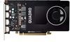
NVIDIA Quadro P2200 vs NVIDIA Quadro P600 Full Specs
1,280 Shaders 1.49GHz | 384 Shaders 1.56GHz |
5GB GDDR5X200.2GB/s | 2GB GDDR564.2GB/s |
·· 3.82 TFLOPS | ·· 1.2 TFLOPS |
Form Factor PCIe Card | Form Factor PCIe Card |
TDP 75W | TDP 40W |
 Quadro P22003.82 TFLOPSFP32
 Quadro P6001.2 TFLOPSFP32
Clock Speed ··· | Clock Speed ··· |
Peak OPS 3.82 TFLOPSFP32 | Peak OPS 1.2 TFLOPSFP32 |
FP32 3.82 TFLOPS | FP32 1.2 TFLOPS |
FP64 119.4 GFLOPS | FP64 37.37 GFLOPS |
Pixel Rate 59.7 GPixel/s | Pixel Rate 24.9 GPixel/s |
Texture Rate 119.4 GTexel/s | Texture Rate 37.4 GTexel/s |
Shaders 1,280 Shaders | Shaders 384 Shaders |
TMUs 80 TMUs | TMUs 24 TMUs |
ROPs 40 ROPs | ROPs 16 ROPs |
SMs 10 SMs | SMs 3 SMs |
Base Clock 1GHz | Base Clock 1.33GHz |
Boost Clock 1.49GHz | Boost Clock 1.56GHz |
L2 Cache 1.5MB shared | L2 Cache 512KB shared |
5GB GDDR5X | 2GB GDDR5 |
Memory Bus 160-bit | Memory Bus 128-bit |
Memory Speed 10GT/s | Memory Speed 4GT/s |
Memory Bandwidth 200.2GB/s | Memory Bandwidth 64.2GB/s |
TDP 75W | TDP 40W |
Multi-Monitor 3 | Multi-Monitor 3 |
4x DisplayPort 1.4 | - |
- | 4x Mini DisplayPort 1.4 |
Encoder Model NVENC 4 | Encoder Model NVENC 4 |
Decoder Model NVDEC 3 | Decoder Model NVDEC 3 |
Form Factor PCIe Card | Form Factor PCIe Card |
PCIe 1-Slots | PCIe 1-Slots |
Height 111 mm (4.37")Width 201 mm (7.91")Depth 20 mm (0.79") | Height 69 mm (2.72")Width 150 mm (5.91")Depth 20 mm (0.79") |
Cooling Blower 1x Fan | Cooling Open-Air 1x Fan |
Manufacturer | Manufacturer |
Chip Designer | Chip Designer |
Architecture | Architecture |
Family | Family |
Branding  | Branding |
Codename NV136 | Codename NV137 |
Chip Variant GP106-300-A1 | Chip Variant GP107-300-A1 |
Market Segment Workstation | Market Segment Workstation |
Release Date Jun 10, 2019 | Release Date Feb 7, 2017 |
Foundry TSMC | Foundry Samsung |
Fabrication Node 16FF | Fabrication Node 14LPP |
Die Size 200mm² | Die Size 132mm² |
Transistor Count 4.4 Billion | Transistor Count 3.3 Billion |
Transistor Density 22 MTr/mm² | Transistor Density 25 MTr/mm² |
No images available
No images available