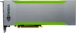
T10
NVIDIA T10 Full Specs
3,072 Shaders 1.4GHz |
16GB GDDR6403.2GB/s |
·· 8.57 TFLOPS |
Form Factor PCIe Card |
TDP 150W |
Power Connectors 1x 8-Pin |
 T10274.3 TOPSINT4 Tensor
3.35 PFLOPS FP4 Tensor SparseGeForce RTX 5090
x12.22Clock Speed ··· |
Peak OPS 274.3 TOPSINT4 Tensor |
Tensor FP16-16 68.57 TFLOPSTensor FP16-32 34.28 TFLOPS |
Tensor BF16 34.28 TFLOPS |
Tensor TF32 34.28 TFLOPS |
FP32 8.57 TFLOPS |
FP64 267.8 GFLOPS |
Tensor INT4 274.3 TOPS |
Tensor INT8 137.1 TOPS |
Ray 25.85 TOPS |
Pixel Rate 133.9 GPixel/s |
Texture Rate 267.8 GTexel/s |
Shaders 3,072 Shaders |
TMUs 192 TMUs |
ROPs 96 ROPs |
Tensor Cores 384 T-Cores |
RT Cores 48 RT-Cores |
SMs 48 SMs |
Base Clock 1.06GHz |
Boost Clock 1.4GHz |
L1 32KB/SM Tex |
L2 Cache 6MB shared |
16GB GDDR6 |
Memory Bus 256-bit |
Memory Speed 12.6GT/s |
Memory Bandwidth 403.2GB/s |
ECC No |
TDP 150W |
Max Resolution 7680x4320 |
Refresh Rate Calculator 7680x4320 Resolution8K UHD Refresh Rate 60Hz |
Adaptive Sync G-Sync FreeSync |
DSC Supported |
Shader Model 6.6 |
DirectX DirectX 12Direct3D 12_2 |
OpenGL 4.6OpenCL 3Vulkan 1.2 |
CUDA 7.5PureVideo HD VP10VDPAU Feature Set J |
Encoder NVENC 7 |
Codec AVC (H.264) HEVC (H.265) |
Decoder NVDEC 4 |
Codec MPEG-1 MPEG-2 MPEG-4 VC-1 VP8 VP9 AVC (H.264) HEVC (H.265) |
Form Factor PCIe Card |
PCIe PCIe 3.0 x16 1-Slots |
Height 111mm (4.37")Width 267mm (10.51")Depth 20mm (0.79") |
Cooling Passive |
Power Connectors 1x 8-Pin |
Multi-GPU Multi-GPU Support SupportedMulti-GPU Type 2-way NVLink |
Foundry TSMC |
Fabrication Node 12FFN |
Die Size 754mm² |
Transistor Count 18.6B |
Transistor Density 24.67 MTr/mm² |