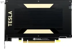
V100 FHHL
NVIDIA V100 FHHL Full Specs
5,120 Shaders 1.29GHz |
16GB HBM2829.4GB/s |
·· 13.21 TFLOPS |
Form Factor PCIe Card |
TDP 250W |
Power Connectors 1x 8-Pin |
 V100 FHHL105.7 TFLOPSFP16-16 Tensor
3.35 PFLOPS FP4 Tensor SparseGeForce RTX 5090
x31.72Clock Speed ··· |
Peak OPS 105.7 TFLOPSFP16-16 Tensor |
Tensor FP16-16 105.7 TFLOPSTensor FP16-32 105.7 TFLOPS |
FP32 13.21 TFLOPS |
FP64 6.61 TFLOPS |
Pixel Rate 165.1 GPixel/s |
Texture Rate 412.8 GTexel/s |
Shaders 5,120 Shaders |
TMUs 320 TMUs |
ROPs 128 ROPs |
Tensor Cores 640 T-Cores |
SMs 80 SMs |
Base Clock 937MHz |
Boost Clock 1.29GHz |
L1 128KB/SM |
L2 Cache 6MB shared |
16GB HBM2 |
Memory Bus 4096-bit |
Memory Speed 1.6GT/s |
Memory Bandwidth 829.4GB/s |
ECC No |
TDP 250W |
Max Resolution 7680x4320 |
Refresh Rate Calculator 7680x4320 Resolution8K UHD Refresh Rate 30Hz |
Adaptive Sync G-Sync FreeSync |
DSC Not Supported |
Shader Model 6.7 |
DirectX DirectX 12Direct3D 12_1 |
OpenGL 4.6OpenCL 3 |
CUDA 7PureVideo HD VP9VDPAU Feature Set I |
Encoder 3x NVENC 5 |
Codec AVC (H.264) HEVC (H.265) |
Decoder NVDEC 3 |
Codec MPEG-1 MPEG-2 MPEG-4 VC-1 VP9 AVC (H.264) HEVC (H.265) |
Form Factor PCIe Card |
PCIe PCIe 3.0 x16 1-Slots |
Height 111mm (4.37")Width 168mm (6.61")Depth 20mm (0.79") |
Cooling Passive |
Power Connectors 1x 8-Pin |
Foundry TSMC |
Fabrication Node 12FFN |
Die Size 815mm² |
Transistor Count 21.1B |
Transistor Density 25.89 MTr/mm² |