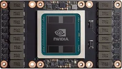
V100 SXM
NVIDIA V100 SXM Full Specs
5,120 Shaders 1.53GHz |
32GB HBM2896GB/s |
·· 15.67 TFLOPS |
Form Factor SXM3 |
TDP 300W |
 V100 SXM125.3 TFLOPSFP16-16 Tensor
3.35 PFLOPS FP4 Tensor SparseGeForce RTX 5090
x26.74Clock Speed ··· |
Peak OPS 125.3 TFLOPSFP16-16 Tensor |
Tensor FP16-16 125.3 TFLOPSTensor FP16-32 125.3 TFLOPS |
FP32 15.67 TFLOPS |
FP64 7.83 TFLOPS |
Pixel Rate 195.8 GPixel/s |
Texture Rate 489.6 GTexel/s |
Shaders 5,120 Shaders |
TMUs 320 TMUs |
ROPs 128 ROPs |
Tensor Cores 640 T-Cores |
SMs 80 SMs |
Base Clock 1.29GHz |
Boost Clock 1.53GHz |
L1 128KB/SM |
L2 Cache 6MB shared |
32GB HBM2 |
Memory Bus 4096-bit |
Memory Speed 1.8GT/s |
Memory Bandwidth 896GB/s |
ECC No |
TDP 300W |
Max Resolution 7680x4320 |
Refresh Rate Calculator 7680x4320 Resolution8K UHD Refresh Rate 30Hz |
Adaptive Sync G-Sync FreeSync |
DSC Not Supported |
Shader Model 6.7 |
DirectX DirectX 12Direct3D 12_1 |
OpenGL 4.6OpenCL 3 |
CUDA 7PureVideo HD VP9VDPAU Feature Set I |
Encoder 3x NVENC 5 |
Codec AVC (H.264) HEVC (H.265) |
Decoder NVDEC 3 |
Codec MPEG-1 MPEG-2 MPEG-4 VC-1 VP9 AVC (H.264) HEVC (H.265) |
Form Factor SXM3 |
PCIe PCIe 3.0 x16 |
Cooling Passive |
Foundry TSMC |
Fabrication Node 12FFN |
Die Size 815mm² |
Transistor Count 21.1B |
Transistor Density 25.89 MTr/mm² |