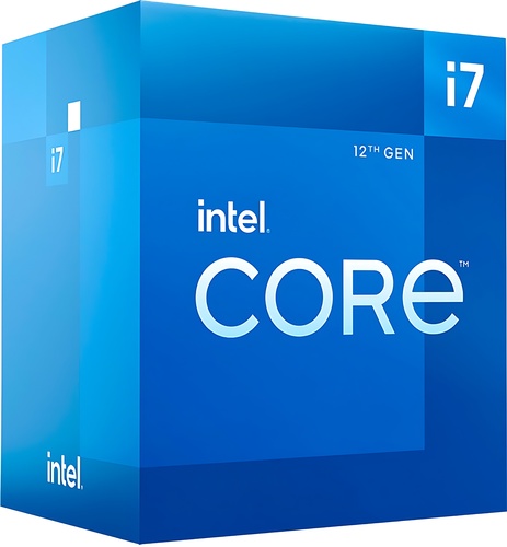
Intel Core i7-12700 vs AMD Ryzen 7 PRO 5750G
Intel Core i7-12700
$370
AMD Ryzen 7 PRO 5750G
|
12 Cores
20 Threads
2.1GHz Clock
|
8 Cores
16 Threads
3.8GHz Clock
|
|
Socket
LGA 1700
|
Socket
AM4
|
|
iGPU
UHD 770 1500MHz
770 GFLOPS FP32
|
iGPU
Radeon Vega 8 2000MHz
2.05 TFLOPS FP32
|
|
GB6S 2,390
59%
|
GB6S 1,970
49%
|
|
GB6M 11,215
42%
|
GB6M 8,300
31%
|
|
CB23S 1,860
72%
|
CB23S 1,490
57%
|
|
CB23M 21,560
50%
|
CB23M 13,700
32%
|
|
Manufacturer
Intel
|
Manufacturer
AMD
|
|
Architecture
Alder Lake
|
Architecture
Zen 2
|
|
Family
Core 12th Gen
|
Family
Ryzen 5000
|
|
Instruction Set (ISA)
x86-64
|
Instruction Set (ISA)
x86-64
|
|
Codename
Alder Lake-S
-
Alder Lake-8P-8E
P-Core
Golden Cove
-
-
E-Core
Gracemont
|
Codename
Cezanne
-
-
-
-
-
-
-
-
|
|
Market Segment
Desktop
|
Market Segment
Desktop
|
|
Release Date
1/18/2022
|
Release Date
6/1/2021
|
|
Foundry
Intel
-
-
-
|
Foundry
TSMC
-
-
-
|
|
Node
Intel 7
-
-
-
|
Node
N7
-
-
-
|
|
Die Size
202 mm²
-
-
-
|
Die Size
180 mm²
-
-
-
|
|
Transistor Count
14.6 Billion
-
-
-
|
Transistor Count
10.7 Billion
-
-
-
|
|
12 Cores
8 P-Cores
-
4 E-Cores
|
8 Cores
-
-
-
|
|
20 Threads
16 P-Threads
-
4 E-Threads
|
16 Threads
-
-
-
|
|
P-Core
2.1GHz
4.9GHz Boost
-
|
-
3.8GHz
4.6GHz Boost
-
|
|
-
-
-
|
-
-
-
|
|
E-Core
1.6GHz
3.6GHz Boost
|
-
-
-
|
|
Overclocking
Locked
-
-
-
|
Overclocking
Locked
-
-
-
|
|
Type
DMI
|
Type
PCIe
|
|
-
-
|
-
-
|
|
-
-
|
-
-
|
|
Transfer Rate
16GT/s
|
Transfer Rate
8GT/s
|
|
-
-
|
-
-
|
|
Lanes
8
|
Lanes
4
|
|
Bandwidth
16GB/s
|
Bandwidth
4GB/s
|
|
Bi-directional
32GB/s
|
Bi-directional
8GB/s
|
|
L0 Instruction
-
-
|
L0 Instruction
-
-
|
|
L0 Data
-
-
|
L0 Data
-
-
|
|
L1 Instruction
32KB/P-Core
8-way set associative
-
-
64KB/E-Core
8-way set associative
|
L1 Instruction
32KB/Core
8-way set associative
-
-
-
-
|
|
L1 Data
48KB/P-Core
12-way set associative
-
-
32KB/E-Core
8-way set associative
|
L1 Data
32KB/Core
8-way set associative
-
-
-
-
|
|
L2
1280KB/Core
10-way set associative
-
-
-
-
-
-
-
-
2MB Shared (E-Core)
16-way set associative
|
L2
512KB/Core
8-way set associative
-
-
-
-
-
-
-
-
-
-
|
|
L3
-
25MB Shared
-
12-way set associative
-
-
-
-
-
|
L3
-
16MB Shared
-
16-way set associative
-
-
-
-
-
|
|
-
-
-
-
|
-
-
-
-
|
|
Channels
2
|
Channels
2
|
|
Max Memory
128GB
128GB
|
Max Memory
128GB
|
|
ECC
Not Supported
|
ECC
Not Supported
|
|
Bus Width/Channel
64Bit
Bus Width
128Bit
|
Bus Width/Channel
64Bit
Bus Width
128Bit
|
|
Clock
2400MHz
1600MHz
Transfer Rate
4800MT/s
3200MT/s
|
Clock
1600MHz
Transfer Rate
3200MT/s
|
|
Bandwidth/Channel
38.4GB/s
25.6GB/s
Bandwidth
76.8GB/s
51.2GB/s
|
Bandwidth/Channel
25.6GB/s
Bandwidth
51.2GB/s
|
|
TDP
65W
-
-
180W Peak
|
TDP
65W
45W cTDP Down
-
-
|
|
Temp
100°C Max
-
|
Temp
95°C Max
-
|
|
Included Cooler
Laminar RM1
|
Included Cooler
Not Included
|
|
PCIe 5.0 x16 Lanes
PCIe 4.0 x4 Lanes
|
PCIe 3.0 x20 Lanes
|
|
UHD 770 1500MHz
256 Shaders
1500MHz
770 GFLOPS FP32
|
Radeon Vega 8 2000MHz
512 Shaders
2000MHz
2.05 TFLOPS FP32
|
|
GNA 3.0
|
No NPU
-
|
|
-
-
|
-
-
|
|
-
|
-
|
|
-
-
|
-
-
|
|
No Cellular
|
No Cellular
|





Copy Link
