AMD Radeon HD 7720 vs NVIDIA GeForce GTX 750
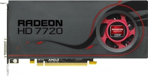
AMD Radeon HD 7720
$149
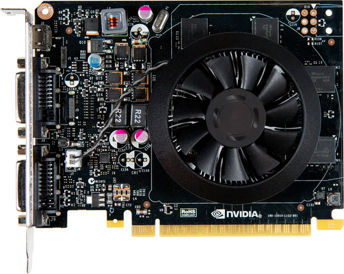
NVIDIA GeForce GTX 750
$119
|
800 Shaders
1GB GDDR5
840MHz
|
512 Shaders
1GB GDDR5
1163MHz
|
|
Peak AI Performance
1.34 TFLOPS
FP32
|
Peak AI Performance
4.76 TOPS
INT8
|
|
FP32
1.34 TFLOPS
|
FP32
1.19 TFLOPS
|
|
-
-
|
-
-
|
|
Form Factor
PCIe Card
2.0-Slots
|
Form Factor
PCIe Card
1.5-Slots
|
|
TDP
150W
|
TDP
55W
|
|
Power Connectors
1x 6-Pin
-
-
-
|
-
-
-
-
-
|
|
GB6 OpenCL N/A
0%
|
|
|
GB6 Metal N/A
0%
|
GB6 Metal N/A
0%
|
|
GB6 Vulkan N/A
0%
|
|
GB5 OpenCL N/A
0%
|
GB5 OpenCL N/A
0%
|
|
GB5 CUDA N/A
0%
|
GB5 CUDA N/A
0%
|
|
GB5 Metal N/A
0%
|
GB5 Metal N/A
0%
|
|
GB5 Vulkan N/A
0%
|
GB5 Vulkan N/A
0%
|
|
OCT 2020.1 N/A
0%
|
OCT 2020.1 N/A
0%
|
|
OCT Metal N/A
0%
|
OCT Metal N/A
0%
|
|
Peak AI
Performance
1.34 TFLOPS
FP32
|
Peak AI
Performance
4.76 TOPS
INT8
|
|
-
-
-
|
-
-
-
|
|
-
-
-
-
-
-
|
-
-
-
-
-
-
|
|
-
-
-
-
-
-
|
-
-
-
-
-
-
|
|
FP32
1.34 TFLOPS
-
-
|
FP32
1.19 TFLOPS
-
-
|
|
-
-
-
|
FP64
40 GFLOPS
-
|
|
-
-
-
-
|
-
-
-
-
|
|
-
-
-
|
-
-
-
|
|
-
-
-
|
-
-
-
|
|
-
-
-
-
|
INT8
4.76 TOPS
-
-
|
|
-
-
|
INT32
1.19 TOPS
|
|
-
-
|
-
-
|
|
Pixel
Fillrate
26.88 GPixel/s
|
Pixel
Fillrate
18.608 GPixel/s
|
|
-
-
|
-
-
|
|
Texture
Fillrate
33.6 GTexel/s
|
Texture
Fillrate
37.216 GTexel/s
|
|
Manufacturer
AMD
|
Manufacturer
NVIDIA
|
|
Chip Designer
AMD
|
Chip Designer
NVIDIA
|
|
Architecture
TeraScale 2
|
Architecture
Maxwell
|
|
Family
Radeon HD 7000
|
Family
GeForce 700
|
|
Codename
Barts
RV940
Variant
Barts LE
|
Codename
NV117
GM107
Variant
GM107-300-A2
|
|
Market Segment
Desktop
|
Market Segment
Desktop
|
|
Release Date
3/15/2013
|
Release Date
2/18/2014
|
|
Foundry
TSMC
-
|
Foundry
TSMC
-
|
|
Fabrication Node
40nm
-
|
Fabrication Node
28nm
-
|
|
Die Size
255 mm²
-
|
Die Size
148 mm²
-
|
|
Transistor Count
1.7 Billion
-
|
Transistor Count
1.9 Billion
-
|
|
Transistor Density
6.67M/mm²
-
|
Transistor Density
12.64M/mm²
-
|
|
Form
PCIe Card
|
Form
PCIe Card
|
|
Shading Units
800 Shaders
-
|
Shading Units
512 Shaders
-
|
|
Texture Mapping Units
40 TMUs
|
Texture Mapping Units
32 TMUs
|
|
Render Output Units
32 ROPs
|
Render Output Units
16 ROPs
|
|
-
-
|
-
-
|
|
-
-
|
-
-
|
|
-
-
|
Streaming Multiprocessors
4 SMs
|
|
Compute Units
10 CUs
|
-
-
|
|
-
-
|
-
-
|
|
-
-
|
-
-
|
|
-
-
-
840MHz
|
-
-
1020MHz Base
1163MHz
|
|
-
-
|
-
-
|
|
L1
-
-
8KB/CU
-
|
L1
-
64KB/SM
-
-
|
|
L2
512KB Shared
|
L2
2MB Shared
|
|
-
-
-
|
-
-
-
|
|
1GB
GDDR5
-
|
1GB
GDDR5
-
|
|
Bus Width
256Bit
|
Bus Width
128Bit
|
|
Clock
1050MHz
Transfer Rate
4.2GT/s
Bandwidth
134.4GB/s
|
Clock
1250MHz
Transfer Rate
5GT/s
Bandwidth
80GB/s
|
|
-
-
-
-
-
-
-
-
-
|
-
-
-
-
-
-
-
-
-
|
|
TDP
150W
|
TDP
55W
|
|
-
-
|
-
-
|
|
-
-
-
-
-
-
-
-
2x DVI-I Dual-Link
-
-
-
-
-
-
-
-
-
-
-
-
1x DisplayPort 1.1
-
-
-
-
-
-
-
-
-
-
-
1x HDMI 1.3
-
-
-
-
-
|
-
-
-
-
-
-
-
-
1x DVI-I Dual-Link
-
1x DVI-D Dual-Link
-
-
-
-
-
-
-
-
-
-
-
-
-
-
-
-
-
1x mini-HDMI 1.4
-
-
-
-
-
-
-
-
-
-
|
|
Max Resolution
2560x1600
|
Max Resolution
4096x2304
|
|
Max Resolution Refresh Rate
60Hz
|
Max Resolution Refresh Rate
30Hz
|
|
Variable Refresh Rate
-
-
-
|
Variable Refresh Rate
G-Sync
FreeSync
-
|
|
Display Stream Compression (DSC)
Not Supported
|
Display Stream Compression (DSC)
Not Supported
|
|
Multi Monitor Support
2
|
Multi Monitor Support
2
|
|
-
-
|
-
-
|
|
No Encoders
-
|
Model
NVENC 2
|
|
-
-
-
-
-
-
-
-
-
-
-
-
-
-
-
|
Codec
-
-
-
-
-
-
-
-
AVC (H.264)
-
-
-
-
-
|
|
Model
UVD 3.0
|
Model
NVDEC 1
|
|
Codec
MPEG-1
MPEG-2
MPEG-4
-
VC-1
-
-
-
AVC (H.264)
-
-
-
-
-
|
Codec
MPEG-1
MPEG-2
MPEG-4
-
VC-1
-
-
-
AVC (H.264)
-
-
-
-
-
|
|
Direct X
11
Direct 3D
11_0
|
Direct X
12
Direct 3D
11_0
|
|
OpenGL
4.5
OpenCL
1.2
-
-
|
OpenGL
4.6
OpenCL
3.0
Vulkan
1.3
|
|
Shader Model
5.0
-
-
GFX
4
-
-
-
-
|
Shader Model
6.7
CUDA
5.0
-
-
PureVideo HD
VP6
VDPAU
Feature Set E
|
|
-
-
-
1x Fan
|
-
-
-
1x Fan
|
|
Power Connectors
-
-
1x 6-Pin
-
-
-
-
|
-
-
-
-
-
-
-
-
|
|
Slots Required
2.0
PCIe Version
2.1
PCIe Lanes
16
|
Slots Required
1.5
PCIe Version
3.0
PCIe Lanes
16
|
|
Multi GPU Support
Supported
Type
4-way CrossFireX
|
-
-
-
-
|
|
Height
111 mm (4.37 in)
Width
198 mm (7.8 in)
Depth
36 mm (1.42 in)
|
Height
111 mm (4.37 in)
Width
145 mm (5.71 in)
Depth
30 mm (1.18 in)
|


Copy Link