AMD Radeon HD 8570 vs AMD Radeon R5 240
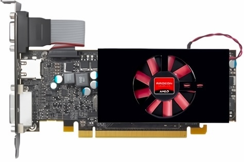
AMD Radeon HD 8570
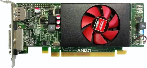
AMD Radeon R5 240
|
384 Shaders
2GB GDDR5
730MHz
|
384 Shaders
1GB GDDR3
780MHz
|
|
Peak AI Performance
560 GFLOPS
FP32
|
Peak AI Performance
600 GFLOPS
FP32
|
|
FP32
560 GFLOPS
|
FP32
600 GFLOPS
|
|
-
-
|
-
-
|
|
Form Factor
PCIe Card
1.0-Slots
|
Form Factor
PCIe Card
1.0-Slots
|
|
TDP
66W
|
TDP
30W
|
|
-
-
-
-
-
|
-
-
-
-
-
|
|
GB6 Metal N/A
0%
|
GB6 Metal N/A
0%
|
|
GB6 Vulkan N/A
0%
|
|
GB5 OpenCL N/A
0%
|
GB5 OpenCL N/A
0%
|
|
GB5 CUDA N/A
0%
|
GB5 CUDA N/A
0%
|
|
GB5 Metal N/A
0%
|
GB5 Metal N/A
0%
|
|
GB5 Vulkan N/A
0%
|
GB5 Vulkan N/A
0%
|
|
OCT 2020.1 N/A
0%
|
OCT 2020.1 N/A
0%
|
|
OCT Metal N/A
0%
|
OCT Metal N/A
0%
|
|
Peak AI
Performance
560 GFLOPS
FP32
|
Peak AI
Performance
600 GFLOPS
FP32
|
|
-
-
-
|
-
-
-
|
|
-
-
-
-
-
-
|
-
-
-
-
-
-
|
|
-
-
-
-
-
-
|
-
-
-
-
-
-
|
|
FP32
560 GFLOPS
-
-
|
FP32
600 GFLOPS
-
-
|
|
FP64
40 GFLOPS
-
|
FP64
40 GFLOPS
-
|
|
-
-
-
-
|
-
-
-
-
|
|
-
-
-
|
-
-
-
|
|
-
-
-
|
-
-
-
|
|
-
-
-
-
|
-
-
-
-
|
|
-
-
|
-
-
|
|
-
-
|
-
-
|
|
Pixel
Fillrate
5.84 GPixel/s
|
Pixel
Fillrate
6.24 GPixel/s
|
|
-
-
|
-
-
|
|
Texture
Fillrate
17.52 GTexel/s
|
Texture
Fillrate
18.72 GTexel/s
|
|
Manufacturer
AMD
|
Manufacturer
AMD
|
|
Chip Designer
AMD
|
Chip Designer
AMD
|
|
Architecture
GCN 1
|
Architecture
GCN 1
|
|
Family
Radeon HD 8000
|
Family
Radeon R 200
|
|
Codename
Oland
-
Variant
Oland XT
|
Codename
Oland
-
Variant
Oland XT
|
|
Market Segment
Desktop
|
Market Segment
Desktop
|
|
Release Date
1/8/2013
|
Release Date
11/1/2013
|
|
Foundry
TSMC
-
|
Foundry
TSMC
-
|
|
Fabrication Node
28nm
-
|
Fabrication Node
28nm
-
|
|
Die Size
77 mm²
-
|
Die Size
90 mm²
-
|
|
Transistor Count
950 Million
-
|
Transistor Count
1 Billion
-
|
|
Transistor Density
12.34M/mm²
-
|
Transistor Density
11.56M/mm²
-
|
|
Form
PCIe Card
|
Form
PCIe Card
|
|
Shading Units
384 Shaders
-
|
Shading Units
384 Shaders
-
|
|
Texture Mapping Units
24 TMUs
|
Texture Mapping Units
24 TMUs
|
|
Render Output Units
8 ROPs
|
Render Output Units
8 ROPs
|
|
-
-
|
-
-
|
|
-
-
|
-
-
|
|
-
-
|
-
-
|
|
Compute Units
6 CUs
|
Compute Units
6 CUs
|
|
-
-
|
-
-
|
|
-
-
|
-
-
|
|
-
-
-
730MHz
|
-
-
730MHz Base
780MHz
|
|
-
-
|
-
-
|
|
L1
-
-
16KB/CU
-
|
L1
-
-
16KB/CU
-
|
|
L2
256KB Shared
|
L2
256KB Shared
|
|
-
-
-
|
-
-
-
|
|
2GB
GDDR5
-
|
1GB
GDDR3
-
|
|
Bus Width
128Bit
|
Bus Width
64Bit
|
|
Clock
1150MHz
Transfer Rate
4.6GT/s
Bandwidth
73.6GB/s
|
Clock
900MHz
Transfer Rate
1.8GT/s
Bandwidth
14.4GB/s
|
|
-
-
-
-
-
-
-
-
-
|
-
-
-
-
-
-
-
-
-
|
|
TDP
66W
|
TDP
30W
|
|
-
-
|
-
-
|
|
-
-
-
-
-
-
-
-
1x DVI-I Dual-Link
-
-
-
-
-
-
-
-
-
-
-
-
-
1x DisplayPort 1.2
-
-
-
-
-
-
-
-
-
-
-
1x HDMI 1.4
-
-
-
-
|
1x VGA
-
-
-
-
-
-
-
1x DVI-I Dual-Link
-
-
-
-
-
-
-
-
-
-
-
-
-
-
-
-
-
-
-
-
-
-
-
-
-
1x HDMI 1.4
-
-
-
-
|
|
Max Resolution
4096x2160
|
Max Resolution
4096x2160
|
|
Max Resolution Refresh Rate
60Hz
|
Max Resolution Refresh Rate
60Hz
|
|
Variable Refresh Rate
-
-
-
|
Variable Refresh Rate
-
-
-
|
|
Display Stream Compression (DSC)
Not Supported
|
Display Stream Compression (DSC)
Not Supported
|
|
Multi Monitor Support
3
|
Multi Monitor Support
3
|
|
-
-
|
-
-
|
|
Model
VCE 1.0
|
Model
VCE 1.0
|
|
Codec
-
-
-
-
-
-
-
-
AVC (H.264)
-
-
-
-
-
|
Codec
-
-
-
-
-
-
-
-
AVC (H.264)
-
-
-
-
-
|
|
Model
UVD 4.0
|
Model
UVD 4.0
|
|
Codec
MPEG-1
MPEG-2
MPEG-4
-
VC-1
-
-
-
AVC (H.264)
-
-
-
-
-
|
Codec
MPEG-1
MPEG-2
MPEG-4
-
VC-1
-
-
-
AVC (H.264)
-
-
-
-
-
|
|
Direct X
12
Direct 3D
11_1
|
Direct X
12
Direct 3D
11_1
|
|
OpenGL
4.6
OpenCL
2.1
Vulkan
1.2
|
OpenGL
4.6
OpenCL
2.1
Vulkan
1.2
|
|
Shader Model
6.5
-
-
GFX
6
-
-
-
-
|
Shader Model
6.5
-
-
GFX
6
-
-
-
-
|
|
-
-
-
1x Fan
|
-
-
-
1x Fan
|
|
-
-
-
-
-
-
-
-
|
-
-
-
-
-
-
-
-
|
|
Slots Required
1.0
PCIe Version
3.0
PCIe Lanes
8
|
Slots Required
1.0
PCIe Version
3.0
PCIe Lanes
8
|
|
Multi GPU Support
Supported
Type
2-way CrossFireX
|
-
-
-
-
|
|
-
-
-
-
-
-
|
-
-
-
-
-
-
|


Copy Link