AMD Radeon R9 285 vs AMD Radeon HD 8950
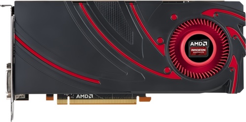
AMD Radeon R9 285
$249

AMD Radeon HD 8950
|
1792 Shaders
2GB GDDR5
918MHz
|
1792 Shaders
3GB GDDR5
925MHz
|
|
Peak AI Performance
3.29 TFLOPS
FP32
|
Peak AI Performance
3.32 TFLOPS
FP32
|
|
FP32
3.29 TFLOPS
|
FP32
3.32 TFLOPS
|
|
-
-
|
-
-
|
|
Form Factor
PCIe Card
2.0-Slots
|
Form Factor
PCIe Card
2.0-Slots
|
|
TDP
190W
|
TDP
225W
|
|
Power Connectors
2x 6-Pin
-
-
-
|
Power Connectors
1x 6-Pin
1x 8-Pin
-
-
|
|
GB6 OpenCL N/A
0%
|
GB6 OpenCL N/A
0%
|
|
GB6 Metal N/A
0%
|
GB6 Metal N/A
0%
|
|
GB6 Vulkan N/A
0%
|
|
GB5 OpenCL N/A
0%
|
GB5 OpenCL N/A
0%
|
|
GB5 CUDA N/A
0%
|
GB5 CUDA N/A
0%
|
|
GB5 Metal N/A
0%
|
GB5 Metal N/A
0%
|
|
GB5 Vulkan N/A
0%
|
GB5 Vulkan N/A
0%
|
|
OCT 2020.1 N/A
0%
|
OCT 2020.1 N/A
0%
|
|
OCT Metal N/A
0%
|
OCT Metal N/A
0%
|
|
Peak AI
Performance
3.29 TFLOPS
FP32
|
Peak AI
Performance
3.32 TFLOPS
FP32
|
|
-
-
-
|
-
-
-
|
|
-
-
-
-
-
-
|
-
-
-
-
-
-
|
|
-
-
-
-
-
-
|
-
-
-
-
-
-
|
|
FP32
3.29 TFLOPS
-
-
|
FP32
3.32 TFLOPS
-
-
|
|
FP64
210 GFLOPS
-
|
FP64
830 GFLOPS
-
|
|
-
-
-
-
|
-
-
-
-
|
|
-
-
-
|
-
-
-
|
|
-
-
-
|
-
-
-
|
|
-
-
-
-
|
-
-
-
-
|
|
-
-
|
-
-
|
|
-
-
|
-
-
|
|
Pixel
Fillrate
29.376 GPixel/s
|
Pixel
Fillrate
29.6 GPixel/s
|
|
-
-
|
-
-
|
|
Texture
Fillrate
102.816 GTexel/s
|
Texture
Fillrate
103.6 GTexel/s
|
|
Manufacturer
AMD
|
Manufacturer
AMD
|
|
Chip Designer
AMD
|
Chip Designer
AMD
|
|
Architecture
GCN 3
|
Architecture
GCN 1
|
|
Family
Radeon R 200
|
Family
Radeon HD 8000
|
|
Codename
Tonga
-
Variant
Tonga Pro
|
Codename
Tahiti
-
Variant
Tahiti Pro
|
|
Market Segment
Desktop
|
Market Segment
Desktop
|
|
Release Date
9/2/2014
|
Release Date
1/8/2013
|
|
Foundry
TSMC
-
|
Foundry
TSMC
-
|
|
Fabrication Node
28nm
-
|
Fabrication Node
28nm
-
|
|
Die Size
359 mm²
-
|
Die Size
352 mm²
-
|
|
Transistor Count
5 Billion
-
|
Transistor Count
4.3 Billion
-
|
|
Transistor Density
13.93M/mm²
-
|
Transistor Density
12.25M/mm²
-
|
|
Form
PCIe Card
|
Form
PCIe Card
|
|
Shading Units
1792 Shaders
-
|
Shading Units
1792 Shaders
-
|
|
Texture Mapping Units
112 TMUs
|
Texture Mapping Units
112 TMUs
|
|
Render Output Units
32 ROPs
|
Render Output Units
32 ROPs
|
|
-
-
|
-
-
|
|
-
-
|
-
-
|
|
-
-
|
-
-
|
|
Compute Units
28 CUs
|
Compute Units
28 CUs
|
|
-
-
|
-
-
|
|
-
-
|
-
-
|
|
-
-
-
918MHz
|
-
-
850MHz Base
925MHz
|
|
-
-
|
-
-
|
|
L1
-
-
16KB/CU
-
|
L1
-
-
16KB/CU
-
|
|
L2
768KB Shared
|
L2
768KB Shared
|
|
-
-
-
|
-
-
-
|
|
2GB
GDDR5
-
|
3GB
GDDR5
-
|
|
Bus Width
256Bit
|
Bus Width
384Bit
|
|
Clock
1375MHz
Transfer Rate
5.5GT/s
Bandwidth
176GB/s
|
Clock
1250MHz
Transfer Rate
5GT/s
Bandwidth
240GB/s
|
|
-
-
-
-
-
-
-
-
-
|
-
-
-
-
-
-
-
-
-
|
|
TDP
190W
|
TDP
225W
|
|
-
-
|
-
-
|
|
-
-
-
-
-
-
-
-
-
-
2x DVI-D Dual-Link
-
-
-
-
-
-
-
-
-
-
-
1x DisplayPort 1.2
-
-
-
-
-
-
-
-
-
-
-
1x HDMI 1.4
-
-
-
-
|
-
-
-
-
-
-
-
-
1x DVI-I Dual-Link
-
-
-
-
-
-
2x mini-DisplayPort 1.2
-
-
-
-
-
-
-
-
-
-
-
-
-
-
-
-
-
-
1x HDMI 1.4
-
-
-
-
|
|
Max Resolution
4096x2160
|
Max Resolution
4096x2160
|
|
Max Resolution Refresh Rate
60Hz
|
Max Resolution Refresh Rate
60Hz
|
|
Variable Refresh Rate
-
FreeSync
-
|
Variable Refresh Rate
-
-
-
|
|
Display Stream Compression (DSC)
Not Supported
|
Display Stream Compression (DSC)
Not Supported
|
|
Multi Monitor Support
3
|
Multi Monitor Support
3
|
|
Content Protection
HDCP 1.4
|
-
-
|
|
Model
VCE 3.0
|
Model
VCE 1.0
|
|
Codec
-
-
-
-
-
-
-
-
AVC (H.264)
HEVC (H.265)
-
-
-
-
|
Codec
-
-
-
-
-
-
-
-
AVC (H.264)
-
-
-
-
-
|
|
Model
UVD 5.0
|
Model
UVD 3.2
|
|
Codec
MPEG-1
MPEG-2
MPEG-4
-
VC-1
-
-
-
AVC (H.264)
-
-
-
-
-
|
Codec
MPEG-1
MPEG-2
MPEG-4
-
VC-1
-
-
-
AVC (H.264)
-
-
-
-
-
|
|
Direct X
12
Direct 3D
12_0
|
Direct X
12
Direct 3D
11_1
|
|
OpenGL
4.6
OpenCL
2.1
Vulkan
1.2
|
OpenGL
4.6
OpenCL
2.1
Vulkan
1.2
|
|
Shader Model
6.5
-
-
GFX
8
-
-
-
-
|
Shader Model
6.5
-
-
GFX
6
-
-
-
-
|
|
-
-
-
1x Fan
|
-
-
-
1x Fan
|
|
Power Connectors
-
-
2x 6-Pin
-
-
-
-
|
Power Connectors
-
-
1x 6-Pin
1x 8-Pin
-
-
-
|
|
Slots Required
2.0
PCIe Version
3.0
PCIe Lanes
16
|
Slots Required
2.0
PCIe Version
3.0
PCIe Lanes
16
|
|
Multi GPU Support
Supported
Type
CrossFire XDMA
|
Multi GPU Support
Supported
Type
4-way CrossFireX
|
|
Height
110 mm (4.33 in)
Width
221 mm (8.7 in)
Depth
36 mm (1.42 in)
|
Height
111 mm (4.37 in)
Width
267 mm (10.51 in)
Depth
38 mm (1.5 in)
|


Copy Link