AMD Radeon R9 285X vs NVIDIA GeForce GTX 770

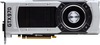
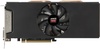
AMD Radeon R9 285X
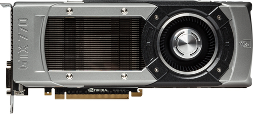
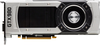
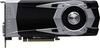
NVIDIA GeForce GTX 770
$399
|
2048 Shaders
3GB GDDR5
1002MHz
|
1536 Shaders
2GB GDDR5
1130MHz
|
|
Peak AI Performance
4.1 TFLOPS
FP32
|
Peak AI Performance
3.47 TOPS
INT32
|
|
FP32
4.1 TFLOPS
|
FP32
3.47 TFLOPS
|
|
-
-
|
-
-
|
|
Form Factor
PCIe Card
2.0-Slots
|
Form Factor
PCIe Card
2.0-Slots
|
|
TDP
200W
|
TDP
230W
|
|
Power Connectors
1x 6-Pin
1x 8-Pin
-
-
|
Power Connectors
2x 6-Pin
-
-
-
|
|
GB6 Metal N/A
0%
|
|
|
GB5 OpenCL N/A
0%
|
GB5 OpenCL N/A
0%
|
|
GB5 CUDA N/A
0%
|
GB5 CUDA N/A
0%
|
|
GB5 Metal N/A
0%
|
GB5 Metal N/A
0%
|
|
GB5 Vulkan N/A
0%
|
GB5 Vulkan N/A
0%
|
|
OCT 2020.1 N/A
0%
|
OCT 2020.1 N/A
0%
|
|
OCT Metal N/A
0%
|
OCT Metal N/A
0%
|
|
Peak AI
Performance
4.1 TFLOPS
FP32
|
Peak AI
Performance
3.47 TOPS
INT32
|
|
-
-
-
|
-
-
-
|
|
-
-
-
-
-
-
|
-
-
-
-
-
-
|
|
-
-
-
-
-
-
|
-
-
-
-
-
-
|
|
FP32
4.1 TFLOPS
-
-
|
FP32
3.47 TFLOPS
-
-
|
|
FP64
260 GFLOPS
-
|
FP64
140 GFLOPS
-
|
|
-
-
-
-
|
-
-
-
-
|
|
-
-
-
|
-
-
-
|
|
-
-
-
|
-
-
-
|
|
-
-
-
-
|
-
-
-
-
|
|
-
-
|
INT32
3.47 TOPS
|
|
-
-
|
-
-
|
|
Pixel
Fillrate
32.064 GPixel/s
|
Pixel
Fillrate
36.16 GPixel/s
|
|
-
-
|
-
-
|
|
Texture
Fillrate
128.256 GTexel/s
|
Texture
Fillrate
144.64 GTexel/s
|
|
Manufacturer
AMD
|
Manufacturer
NVIDIA
|
|
Chip Designer
AMD
|
Chip Designer
NVIDIA
|
|
Architecture
GCN 3
|
Architecture
Kepler
|
|
Family
Radeon R 200
|
Family
GeForce 700
|
|
Codename
Tonga
-
Variant
Tonga XT
|
Codename
NVE4
GK104
Variant
GK104-425-A2
|
|
Market Segment
Desktop
|
Market Segment
Desktop
|
|
Release Date
9/2/2014
|
Release Date
5/30/2013
|
|
Foundry
TSMC
-
|
Foundry
TSMC
-
|
|
Fabrication Node
28nm
-
|
Fabrication Node
28nm
-
|
|
Die Size
359 mm²
-
|
Die Size
294 mm²
-
|
|
Transistor Count
5 Billion
-
|
Transistor Count
3.5 Billion
-
|
|
Transistor Density
13.93M/mm²
-
|
Transistor Density
12.04M/mm²
-
|
|
Form
PCIe Card
|
Form
PCIe Card
|
|
Shading Units
2048 Shaders
-
|
Shading Units
1536 Shaders
-
|
|
Texture Mapping Units
128 TMUs
|
Texture Mapping Units
128 TMUs
|
|
Render Output Units
32 ROPs
|
Render Output Units
32 ROPs
|
|
-
-
|
-
-
|
|
-
-
|
-
-
|
|
-
-
|
Streaming Multiprocessors
8 SMs
|
|
Compute Units
32 CUs
|
-
-
|
|
-
-
|
-
-
|
|
-
-
|
-
-
|
|
-
-
-
1002MHz
|
-
-
1046MHz Base
1130MHz
|
|
-
-
|
-
-
|
|
L1
-
-
16KB/CU
-
|
L1
48KB/SM Tex
16KB/SM
-
-
|
|
L2
768KB Shared
|
L2
512KB Shared
|
|
-
-
-
|
-
-
-
|
|
3GB
GDDR5
-
|
2GB
GDDR5
-
|
|
Bus Width
384Bit
|
Bus Width
256Bit
|
|
Clock
1375MHz
Transfer Rate
5.5GT/s
Bandwidth
264GB/s
|
Clock
1753MHz
Transfer Rate
7GT/s
Bandwidth
224.3GB/s
|
|
-
-
-
-
-
-
-
-
-
|
-
-
-
-
-
-
-
-
-
|
|
TDP
200W
|
TDP
230W
|
|
-
-
|
-
-
|
|
-
-
-
-
-
-
-
-
-
-
2x DVI-D Dual-Link
-
-
-
-
-
-
-
-
-
-
-
1x DisplayPort 1.2
-
-
-
-
-
-
-
-
-
-
-
1x HDMI 1.4
-
-
-
-
|
-
-
-
-
-
-
-
-
1x DVI-I Dual-Link
-
1x DVI-D Dual-Link
-
-
-
-
-
-
-
-
-
-
-
1x DisplayPort 1.2
-
-
-
-
-
-
-
-
-
-
-
1x HDMI 1.4
-
-
-
-
|
|
Max Resolution
4096x2160
|
Max Resolution
4096x2304
|
|
Max Resolution Refresh Rate
60Hz
|
Max Resolution Refresh Rate
60Hz
|
|
Variable Refresh Rate
-
FreeSync
-
|
Variable Refresh Rate
G-Sync
FreeSync
-
|
|
Display Stream Compression (DSC)
Not Supported
|
Display Stream Compression (DSC)
Not Supported
|
|
Multi Monitor Support
3
|
Multi Monitor Support
2
|
|
Content Protection
HDCP 1.4
|
-
-
|
|
Model
VCE 3.0
|
Model
NVENC 1
|
|
Codec
-
-
-
-
-
-
-
-
AVC (H.264)
HEVC (H.265)
-
-
-
-
|
Codec
-
-
-
-
-
-
-
-
AVC (H.264)
-
-
-
-
-
|
|
Model
UVD 5.0
|
Model
NVDEC 1
|
|
Codec
MPEG-1
MPEG-2
MPEG-4
-
VC-1
-
-
-
AVC (H.264)
-
-
-
-
-
|
Codec
MPEG-1
MPEG-2
MPEG-4
-
VC-1
-
-
-
AVC (H.264)
-
-
-
-
-
|
|
Direct X
12
Direct 3D
12_0
|
Direct X
12
Direct 3D
11_0
|
|
OpenGL
4.6
OpenCL
2.1
Vulkan
1.2
|
OpenGL
4.6
OpenCL
3.0
Vulkan
1.2
|
|
Shader Model
6.5
-
-
GFX
8
-
-
-
-
|
Shader Model
6.5
CUDA
3.0
-
-
PureVideo HD
VP5
VDPAU
Feature Set D
|
|
-
-
-
1x Fan
|
-
-
-
1x Fan
|
|
Power Connectors
-
-
1x 6-Pin
1x 8-Pin
-
-
-
|
Power Connectors
-
-
2x 6-Pin
-
-
-
-
|
|
Slots Required
2.0
PCIe Version
3.0
PCIe Lanes
16
|
Slots Required
2.0
PCIe Version
3.0
PCIe Lanes
16
|
|
Multi GPU Support
Supported
Type
CrossFire XDMA
|
Multi GPU Support
Supported
Type
4-way SLI
|
|
Height
110 mm (4.33 in)
Width
267 mm (10.51 in)
Depth
37 mm (1.46 in)
|
Height
111 mm (4.37 in)
Width
267 mm (10.51 in)
Depth
38 mm (1.5 in)
|


Copy Link